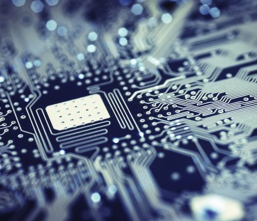
An Automated Test Equipment PCB is a critical component used in ATE systems to perform functional, parametric, and reliability testing of semiconductor devices. These PCBs serve as the electrical interface between the test system and the device under test (DUT), ensuring accurate signal transmission, stable power delivery, and reliable measurement during high-volume semiconductor testing.
As semiconductor devices evolve toward higher speeds, higher integration, and mixed-signal architectures, the design and manufacturing requirements for automated test equipment PCBs have become increasingly demanding. Precision, repeatability, and long-term reliability are essential for modern ATE environments.
Key Design Requirements of Automated Test Equipment PCBs
1. High Pin Count and Dense Routing Capability
ATE PCBs must support devices with hundreds or thousands of I/O connections. High-density routing, HDI structures, and multilayer stackups enable efficient signal fan-out while maintaining electrical integrity.
2. Controlled Impedance and Signal Integrity
High-speed digital and RF testing requires strict controlled impedance PCB design. Accurate impedance control reduces signal reflection, jitter, and loss during test operations.
3. Power Integrity and Noise Suppression
Stable power delivery is critical for accurate measurements. Optimized power planes, decoupling networks, and low-impedance PDN design minimize voltage fluctuations and electrical noise.
4. Mixed-Signal Isolation and Grounding
ATE PCBs often test devices with analog, digital, and RF functions. Proper grounding, shielding, and isolation techniques reduce crosstalk and electromagnetic interference.
5. Mechanical Accuracy and Durability
ATE PCBs must withstand frequent handling, repeated socket insertions, and long test cycles. Mechanical robustness ensures consistent performance over extended operational lifetimes.
Applications of Automated Test Equipment PCBs
Automated test equipment PCBs are widely used in:
-
Logic IC and microprocessor testing
-
Memory and storage device testing
-
RF and wireless semiconductor validation
-
Power management and analog IC testing
-
Automotive, industrial, and aerospace semiconductor testing
These applications require high accuracy, repeatability, and throughput.
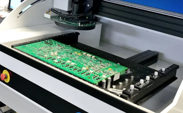
Manufacturing Capabilities for Automated Test Equipment PCBs
Reliable ATE PCBs require advanced manufacturing capabilities, including:
-
HDI and high-layer-count PCB fabrication
-
Controlled impedance manufacturing and verification
-
Fine-line etching and precision drilling
-
High-Tg and low-loss laminate processing
-
Prototype, small batch, and mass production support
Consistent manufacturing quality ensures stable test performance across different test platforms.
Why Automated Test Equipment PCB Quality Matters
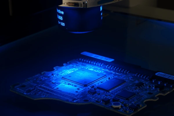
Low-quality ATE PCBs can cause signal distortion, power noise, and measurement instability, leading to inaccurate test results and reduced yield. High-quality automated test equipment PCBs provide:
-
Accurate and repeatable measurements
-
Reduced test downtime and maintenance
-
Improved ATE efficiency and throughput
-
Reliable semiconductor validation
Conclusion
The Automated Test Equipment PCB is the backbone of modern semiconductor testing, enabling precise and reliable validation of advanced ICs. Through HDI routing, controlled impedance design, robust power integrity, and high-quality manufacturing, ATE PCBs ensure consistent performance in high-speed, high-volume test environments.
Choosing an experienced automated test equipment PCB manufacturer helps improve test accuracy, accelerate product qualification, and support long-term semiconductor production success.
