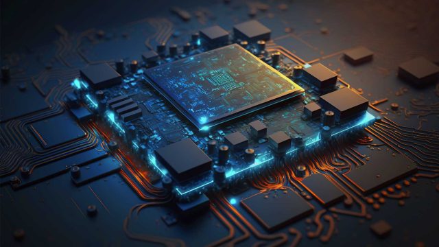
A Chip Test PCB is a specialized semiconductor test board used in Automated Test Equipment (ATE) to verify the electrical performance, functionality, and reliability of semiconductor chips before mass production. These PCBs play a critical role in chip validation, characterization, and production testing, ensuring that ICs meet performance and quality requirements.
As semiconductor chips continue to evolve toward higher speed, higher integration, and smaller geometries, the requirements for chip test PCB design and manufacturing have become increasingly demanding. High pin count, fine pitch packages, and mixed-signal architectures require precise PCB engineering and manufacturing control.
Key Design Requirements of Chip Test PCBs
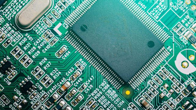
1. High Pin Count and Dense Routing Capability
Modern chips often feature hundreds or thousands of I/O pins. Chip test PCBs must support high pin count layouts using HDI technology, fine-line routing, and multilayer stackups to ensure accurate signal access.
2. Controlled Impedance and Signal Integrity
High-speed digital, RF, and high-frequency signals require strict controlled impedance PCB design. Proper impedance control minimizes reflection, jitter, and signal loss during chip testing.
3. Power Integrity and Noise Control
Stable power delivery is essential for reliable chip testing. Optimized power and ground planes, decoupling strategies, and low-impedance PDN design ensure consistent and repeatable measurements.
4. Mixed-Signal Isolation
Many chips integrate analog, digital, and RF circuits on a single die. Effective grounding and isolation techniques reduce crosstalk and electromagnetic interference on the chip test PCB.
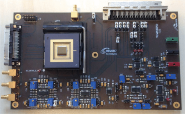
5. Mechanical Accuracy and Socket Compatibility
Chip test PCBs must align precisely with test sockets, probe cards, or load boards, maintaining reliable contact over repeated insertion cycles.
Applications of Chip Test PCBs
Chip test PCBs are widely used for testing:
-
Logic ICs and microprocessors
-
Memory chips (DRAM, NAND, Flash)
-
RF and wireless communication chips
-
Power management ICs (PMICs)
-
Mixed-signal and sensor ICs
These applications demand high accuracy, repeatability, and long-term stability in semiconductor testing environments.
Manufacturing Capabilities for Chip Test PCBs
Producing high-performance chip test PCBs requires advanced manufacturing capabilities, including:
-
HDI and high-layer-count PCB fabrication
-
Controlled impedance manufacturing and verification
-
Fine-pitch drilling and precision etching
-
High-Tg and low-loss laminate processing
-
Prototype, small batch, and volume production support
Consistent manufacturing quality ensures reliable test performance across different production runs.
Why Chip Test PCB Quality Matters
A poorly designed chip test PCB can introduce measurement errors, signal distortion, and test instability, directly impacting chip yield and reliability qualification. High-quality chip test PCBs provide:
-
Accurate and repeatable test results
-
Reduced test downtime and maintenance
-
Improved ATE efficiency and throughput
-
Reliable chip validation for mass production
Conclusion
The Chip Test PCB is a critical foundation of semiconductor testing, enabling precise validation of modern high-speed, high-integration chips. Through HDI routing, controlled impedance design, optimized power integrity, and robust manufacturing, chip test PCBs support accurate, stable, and repeatable semiconductor testing.
Working with an experienced chip test PCB manufacturer ensures consistent quality, faster development cycles, and reliable performance throughout the semiconductor product lifecycle.
