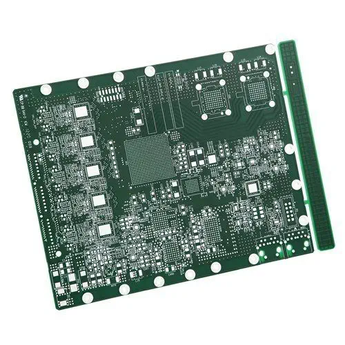
As semiconductor devices become more complex with increasing pin counts and high-speed signal requirements, high layer count ATE PCBs have become essential for accurate automated test equipment (ATE) operation. These multilayer boards enable dense routing, controlled impedance, and reliable signal integrity, ensuring precise and repeatable semiconductor testing.
High layer count ATE PCBs allow engineers to test advanced ICs, wafer-level devices, and high-speed modules efficiently, while maintaining mechanical stability and electrical performance.
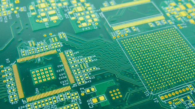
What Is a High Layer Count ATE PCB?
A high layer count ATE PCB is a printed circuit board designed for automated semiconductor testing that uses multiple layers to accommodate complex routing, high-density connections, and robust power and ground distribution. Its key roles include:
-
Supporting high pin count ICs for functional validation
-
Maintaining signal integrity across high-speed or RF channels
-
Providing controlled impedance and low-loss routing
-
Enabling compact layouts for advanced ATE test fixtures
By increasing the number of layers, engineers can route dense signals while maintaining reliability and performance.
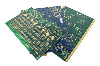
Key Features of High Layer Count ATE PCBs
-
Multilayer Routing – Enables high-density signal paths for complex IC packages and probe card interfaces.
-
Controlled Impedance – Maintains signal integrity for high-speed and high-frequency testing.
-
High Pin Count Support – Efficiently breaks out connections for advanced ICs and load boards.
-
Power and Ground Management – Multiple planes reduce noise and voltage fluctuations during testing.
-
Mechanical Stability – Rigid construction ensures alignment and reliability during repeated test cycles.
These features ensure accurate semiconductor validation and minimize signal distortion.
Material and Stackup Considerations
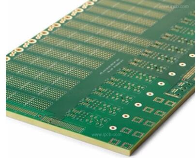
High layer count ATE PCBs require careful material selection and stackup planning:
-
High-Tg FR-4 or Low-Loss Laminates – Provide thermal stability and high-frequency performance.
-
Optimized Multilayer Stackups – Balance signal integrity, impedance control, and manufacturability.
-
Hybrid Stackups – May combine standard and low-loss materials for cost-efficient high-performance testing.
Proper design ensures repeatable, high-quality results in both prototype and production environments.
Applications of High Layer Count ATE PCBs
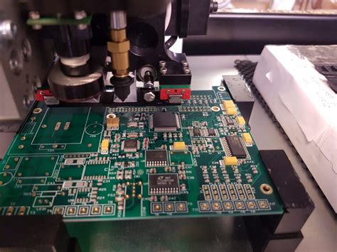
High layer count ATE PCBs are widely used in:
-
Semiconductor IC functional and parametric testing
-
Wafer-level testing and probe card integration
-
Load boards for ATE systems
-
High-speed digital, RF, and mixed-signal IC validation
They are particularly critical for modern ICs with dense pin counts and complex functionality.
Choosing a High Layer Count ATE PCB Manufacturer
When selecting a high layer count ATE PCB supplier, consider:
-
Experience with multilayer, high pin count, and high-speed test boards
-
Capability for controlled impedance and low-loss routing
-
Support for prototype, small batch, and volume production
-
Quality control and electrical verification procedures
A professional partner ensures precise signal integrity, repeatable performance, and reliable ATE operation.
Conclusion
High layer count ATE PCBs are crucial for modern semiconductor testing, providing multilayer routing, controlled impedance, and mechanical stability for high-speed, high-density IC validation. By partnering with an experienced high layer count ATE PCB manufacturer, engineers can ensure reliable test results, faster prototyping, and smooth transition to mass production.
