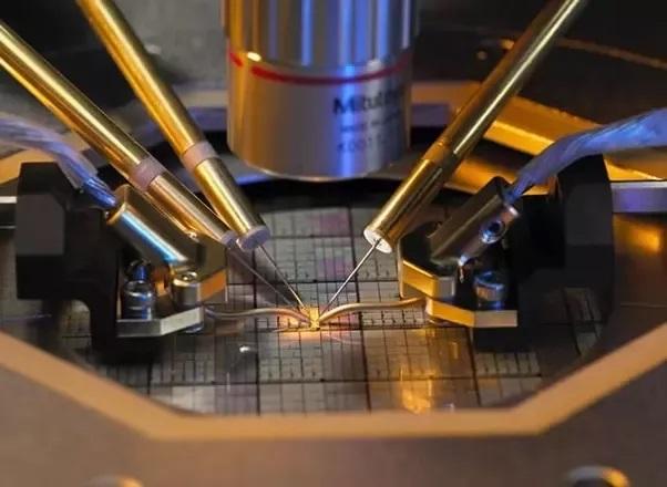
In semiconductor manufacturing, wafer-level testing is a critical step to ensure device functionality and yield before packaging. Wafer Test PCBs serve as the interface between wafers and automated test equipment (ATE), enabling precise electrical measurement and reliable characterization across high-density IC arrays.
These specialized PCBs are designed for controlled impedance, high pin count, and high-frequency performance, making them essential in modern IC wafer testing workflows.
What Is a Wafer Test PCB?
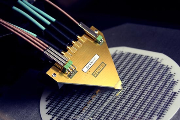
A Wafer Test PCB is a custom printed circuit board engineered for probing and testing semiconductor wafers. It is typically used with probe cards or wafer handling fixtures to connect multiple dies simultaneously to ATE systems for functional and parametric testing.
Key characteristics include:
-
High-density routing for large IC arrays
-
Controlled impedance for signal integrity
-
Stable power distribution across all test points
-
Mechanical durability for repeated probe cycles
Key Design Considerations
Designing a Wafer Test PCB requires careful attention to:
-
Signal Integrity: Minimize reflections, crosstalk, and insertion loss for accurate measurements.
-
Controlled Impedance: Maintain precise impedance for high-speed wafer-level signals.
-
High-Density Routing: Break out thousands of IC pins efficiently.
-
Mechanical Reliability: Ensure robust performance under repeated probing and thermal cycling.
These factors ensure repeatable test results and reduce wafer test failures.
Materials and Stackup
Wafer Test PCBs often use low-loss laminates or hybrid materials to support high-frequency signals and long-term reliability. Stackups are designed to:
-
Provide consistent reference planes
-
Minimize signal skew between layers
-
Support multilayer routing for dense IC arrays
Proper material selection and stackup design are critical for high-quality wafer testing.
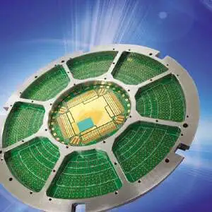
Applications of Wafer Test PCBs
Wafer Test PCBs are essential in:
-
Wafer-level functional and parametric testing
-
High-speed IC characterization
-
Probe card interfaces for ATE systems
-
High-density semiconductor device evaluation
Each application relies on precision, reliability, and consistent electrical performance.
Choosing a Wafer Test PCB Manufacturer

When selecting a Wafer Test PCB supplier, consider:
-
Experience in high-density, high-speed semiconductor PCBs
-
Capability for controlled impedance and multilayer designs
-
Prototyping and small-batch production support
-
Advanced testing and quality assurance processes
A reliable manufacturer ensures accurate wafer testing and repeatable results.
Conclusion
The Wafer Test PCB is a cornerstone of semiconductor manufacturing, providing precise electrical interfaces for wafer-level testing. By combining high-density routing, controlled impedance, and robust mechanical design, these PCBs enable reliable and accurate IC validation. Partnering with an experienced Wafer Test PCB manufacturer ensures performance, repeatability, and confidence in semiconductor testing workflows.
