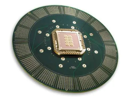
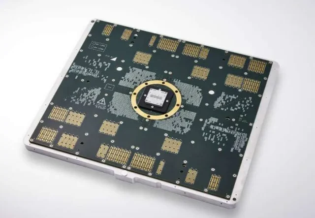
In wafer-level semiconductor testing, probe cards must deliver precise electrical contact across thousands of touchdowns while maintaining consistent signal performance. The Custom Probe Card PCB provides the structural and electrical foundation that supports probe arrays, ensuring accurate, repeatable wafer testing.
A properly engineered custom probe card PCB directly impacts test yield, device characterization accuracy, and probe lifetime.
Why Probe Card PCBs Must Be Custom Designed
Every wafer test application differs in:
-
Pad pitch and layout
-
Signal type and frequency
-
Mechanical alignment requirements
A custom probe card PCB is tailored to match exact wafer and tester specifications, ensuring precise probe-to-pad contact.
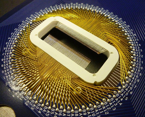
Precision Routing for Dense Probe Interfaces
Custom probe card PCBs often require:
-
Ultra-fine trace width and spacing
-
High-density interconnect (HDI) structures
-
Controlled fan-out from probe contact points
These capabilities enable dense signal routing without compromising reliability.
Signal Integrity at the Probe-to-PCB Transition
Signal degradation at the interface can distort measurements. Custom probe card PCBs are designed to:
-
Maintain controlled impedance
-
Minimize parasitic capacitance and inductance
-
Reduce reflection at high frequencies
Clean signal transitions improve measurement accuracy.
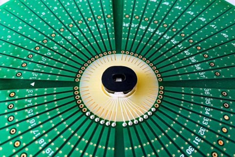
Grounding Strategy and Noise Control
To suppress noise and crosstalk, probe card PCBs incorporate:
-
Dedicated ground planes
-
Ground shielding around sensitive channels
-
Via stitching near high-speed paths
Effective grounding improves test repeatability.
Mechanical Flatness and Structural Stability
Probe card PCBs must maintain:
-
Tight flatness tolerances
-
Dimensional stability during temperature cycling
-
Mechanical robustness under repeated probing
These factors directly affect probe alignment and contact reliability.
Material Selection for Precision and Durability
Custom probe card PCBs may use:
-
High-Tg FR-4 for mechanical strength
-
Low-CTE laminates for dimensional control
-
Hybrid materials for high-frequency test applications
Material choice influences both electrical and mechanical performance.
Manufacturing Accuracy and Inspection
Fabrication requires:
-
Precise layer-to-layer registration
-
Reliable microvia formation
-
Advanced inspection and electrical testing
Strict process control ensures consistent quality.
Applications of Custom Probe Card PCBs
Custom probe card PCBs are used in:
-
Wafer-level parametric testing
-
High-frequency and mixed-signal device testing
-
Logic, memory, and advanced node IC testing
-
Engineering validation and production screening
Each application demands extreme precision.
Selecting a Custom Probe Card PCB Manufacturer
When choosing a custom probe card PCB supplier, look for:
-
Experience with wafer test hardware
-
HDI and fine-line fabrication capability
-
Controlled impedance expertise
-
Support for prototype and low-volume production
An experienced partner improves yield and probe lifespan.
Conclusion
The Custom Probe Card PCB is a critical enabler of accurate and repeatable wafer-level testing. Through precision routing, stable mechanical design, and controlled electrical performance, custom probe card PCBs support high-yield semiconductor manufacturing.
Working with a specialized custom probe card PCB manufacturer ensures reliable wafer testing from development through production.
