Automated Test Equipment (ATE) platforms are highly configurable, but their performance ultimately depends on how well the test interface matches the device under test. A Custom ATE PCB is specifically designed to bridge this gap by aligning electrical, mechanical, and system-level requirements for accurate and repeatable semiconductor testing.
Unlike off-the-shelf boards, a custom ATE PCB is engineered to optimize test performance for a specific application.
What Is a Custom ATE PCB?
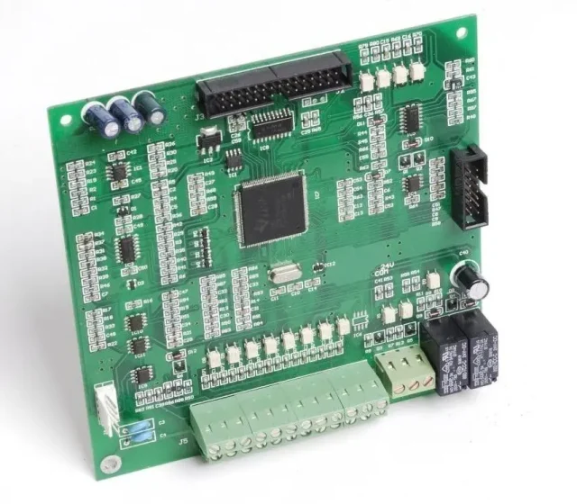
A Custom ATE PCB is a purpose-built printed circuit board designed to interface a specific ATE system with a particular device or device family. It may integrate:
-
Device-specific sockets or fixtures
-
Controlled impedance signal routing
-
Customized power and grounding networks
Custom ATE PCBs are tailored to meet precise electrical and mechanical test requirements.
Why Customization Matters in ATE Testing
Standard interfaces often fail to account for:
-
Unique signal speed and timing requirements
-
Specialized power sequencing and current demand
-
Mechanical constraints of device packages
A Custom ATE PCB ensures the test environment accurately reflects real operating conditions.
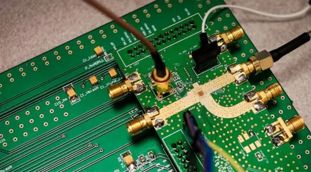
Signal Integrity Optimization for Custom ATE PCBs
High-speed testing requires careful signal path control. Custom ATE PCB designs incorporate:
-
Impedance-controlled transmission lines
-
Length matching for timing-critical signals
-
Optimized return path and reference plane design
These features minimize measurement distortion and timing errors.
Power Integrity and Load Management
Different devices place different demands on power delivery. A Custom ATE PCB allows:
-
Device-specific power plane design
-
Optimized decoupling capacitor placement
-
Low-noise grounding strategies
Stable power delivery improves test accuracy and reduces false failures.
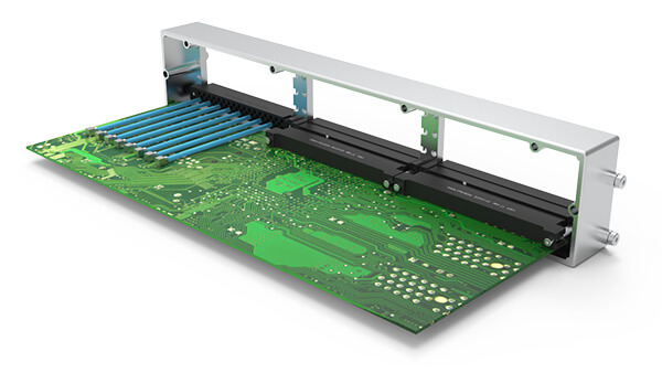
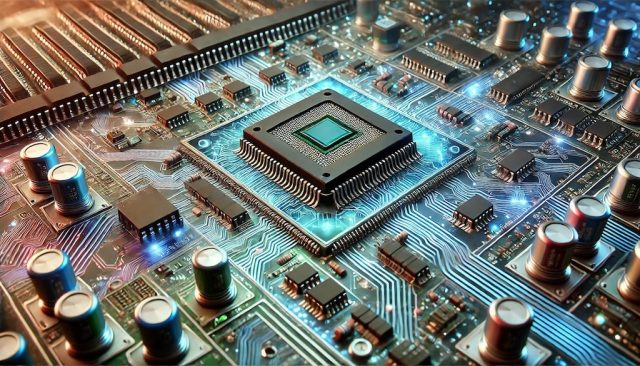
High Pin Count and Complex Interface Support
Modern ICs often require hundreds or thousands of test connections. Custom ATE PCBs support:
-
High pin count routing
-
Fine-pitch socket integration
-
Multilayer and HDI PCB technologies
Custom routing ensures clean signal paths even in dense designs.
Mechanical Design and Reliability
Mechanical precision is critical for long-term testing. Custom ATE PCBs are designed with:
-
Reinforced socket mounting areas
-
Tight flatness and coplanarity control
-
Balanced stackup to reduce warpage
Mechanical stability supports consistent electrical contact.
Material and Stackup Selection
Custom ATE PCBs allow flexibility in material choice:
-
High-Tg FR-4 for durability
-
Low-loss laminates for high-speed signals
-
Hybrid stackups for mixed-signal systems
Material selection is optimized for the test environment.
Manufacturing Consistency and Validation
Because ATE PCBs are used in production testing, consistency is essential. Custom ATE PCBs require:
-
Tight manufacturing tolerances
-
Electrical and impedance verification
-
Process traceability across builds
Reliable manufacturing ensures consistent test results.
Typical Applications of Custom ATE PCBs
Custom ATE PCBs are widely used in:
-
Semiconductor final test
-
System-level test (SLT)
-
Automotive and industrial IC qualification
-
High-speed logic, memory, and mixed-signal devices
Each application benefits from tailored test interfaces.
Choosing a Custom ATE PCB Manufacturing Partner
When selecting a Custom ATE PCB manufacturer, key considerations include:
-
Experience with ATE platforms and test requirements
-
High pin count and controlled impedance capability
-
Strong engineering support for customization
-
Proven quality and process consistency
A knowledgeable partner helps reduce test risk and development time.
Conclusion
The Custom ATE PCB is a critical component for achieving accurate, repeatable, and scalable semiconductor testing. By tailoring signal routing, power delivery, mechanical structure, and materials to specific test needs, custom ATE PCBs enable reliable validation from engineering development to mass production.
Partnering with an experienced Custom ATE PCB supplier ensures stable test performance and long-term production success.
