As electronic devices and semiconductor systems grow more complex, test requirements evolve beyond what simple PCB structures can support. The Multilayer Test PCB provides the routing density, electrical isolation, and power stability required for accurate, repeatable testing across development and production stages.
A professionally engineered Multilayer Test PCB ensures that test results remain consistent as designs scale in speed, pin count, and functionality.
What Is a Multilayer Test PCB?
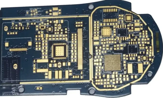
A Multilayer Test PCB is a specialized printed circuit board constructed with multiple conductive layers to support high-density signal routing and robust power distribution in test environments. It is commonly used to interface:
-
Test equipment and instruments
-
Devices under test (DUTs)
-
Sockets, fixtures, or probe interfaces
Unlike standard application PCBs, multilayer test PCBs prioritize measurement stability and test repeatability.
Why Multilayer Structure Matters in Test PCBs
Multi-layer construction enables:
-
Separation of signal, power, and ground layers
-
Reduced electromagnetic interference (EMI)
-
Improved signal isolation and integrity
These benefits are critical when testing high-speed, high-pin-count devices.
Signal Integrity in Multilayer Test PCBs
High-speed testing requires clean, predictable signal paths. Effective Multilayer Test PCB designs incorporate:
-
Controlled impedance traces
-
Dedicated reference planes adjacent to signal layers
-
Short, well-matched routing paths
These measures reduce crosstalk, reflections, and timing skew during testing.
Power Integrity and Grounding Strategy

Test environments demand stable power delivery. Multilayer test PCBs support:
-
Low-impedance power planes
-
Multiple voltage domains
-
Optimized decoupling capacitor placement
Proper grounding and plane coupling help minimize noise that can affect test accuracy.
High Pin Count and Routing Density
Testing advanced devices often requires hundreds or thousands of connections. A Multilayer Test PCB enables:
-
Efficient breakout from dense pin fields
-
Support for fine-pitch connectors and sockets
-
Integration of HDI features where necessary
Layer count is often increased to maintain routing quality without compromising performance.
Mechanical Stability and Stackup Balance
Mechanical reliability is essential for repeatable testing. Multilayer test PCBs are designed with:
-
Symmetrical stackups to reduce warpage
-
Reinforced connector and socket mounting areas
-
Tight flatness and coplanarity control
Mechanical stability ensures consistent electrical contact throughout test cycles.
Materials and Stackup Selection
Material choice affects both electrical and mechanical performance:
-
High-Tg FR-4 for durability
-
Low-loss laminates for high-speed signal layers
-
Hybrid stackups for mixed-frequency test systems
Careful stackup design ensures stable performance across temperature and time.
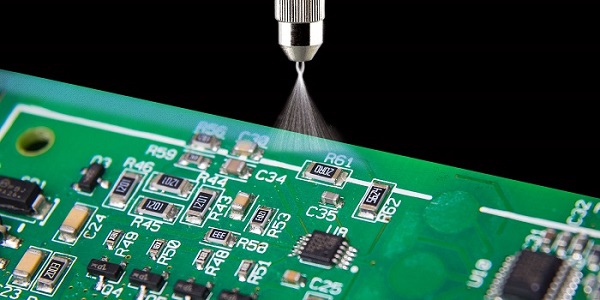
Manufacturing Precision and Quality Control
Multilayer test PCBs require strict manufacturing discipline:
-
Accurate layer registration
-
Reliable via drilling and plating
-
Electrical continuity and impedance verification
Consistent manufacturing quality is essential for reproducible test results.
Typical Applications of Multilayer Test PCBs

Multilayer Test PCBs are widely used in:
-
Semiconductor test hardware
-
High-speed digital and mixed-signal testing
-
Automotive and industrial electronics validation
-
RF and communication system testing
These applications rely on stable, repeatable electrical interfaces.
Choosing a Multilayer Test PCB Manufacturing Partner
When selecting a Multilayer Test PCB manufacturer, key considerations include:
-
Experience with complex multilayer test boards
-
Controlled impedance and high pin count capability
-
Strong process consistency and traceability
-
Engineering support for rapid test board iteration
A reliable partner helps ensure smooth transitions from validation to production.
Conclusion
The Multilayer Test PCB is a foundational platform for advanced electronic testing, enabling high routing density, robust power integrity, and consistent test performance. By combining thoughtful stackup design, precise manufacturing, and reliable materials, multilayer test PCBs support accurate testing throughout the product lifecycle.
Partnering with an experienced Multilayer Test PCB supplier is essential for achieving reliable and repeatable test results.
