As semiconductor devices continue to scale down in size while increasing in performance, wafer-level testing demands extreme precision. At the heart of this process lies the Probe Card PCB, a critical platform that connects automated test equipment to microscopic probe needles touching individual die pads.
A professionally manufactured Probe Card PCB directly determines probing accuracy, contact repeatability, and overall test yield.
What Is a Probe Card PCB?
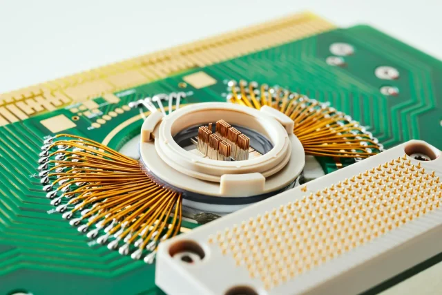
A Probe Card PCB is a highly specialized printed circuit board used in wafer probing systems. It serves as the electrical and mechanical foundation that supports:
-
Probe needles or MEMS probes
-
High-density interconnections
-
Signal routing between wafer pads and ATE systems
Unlike standard PCBs, probe card PCBs must operate with micron-level alignment accuracy and maintain electrical stability under repeated mechanical contact.
Why Probe Card PCB Quality Matters
In wafer-level testing, even minimal PCB deviation can cause:
-
Unstable probe contact resistance
-
Measurement noise and signal distortion
-
Increased false failures or test escapes
A high-quality Probe Card PCB ensures that each probe contact behaves consistently across thousands of touchdown cycles.
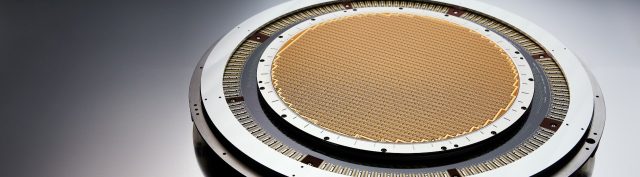
High Pin Count and Fine-Pitch Challenges
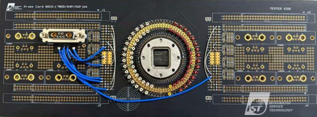
Modern ICs often require thousands of test points with extremely tight spacing. A Probe Card PCB must support:
-
Ultra-high pin count routing
-
Fine-line and fine-pitch trace geometry
-
Accurate pad positioning and planarity
Advanced HDI technology is often required to meet these demands.
Signal Integrity in Probe Card PCBs
As test frequencies rise, Probe Card PCB signal integrity becomes critical. Key design considerations include:
-
Controlled impedance routing
-
Minimized trace length variation
-
Optimized return path design
These factors help reduce reflections, crosstalk, and timing errors during high-speed wafer testing.
Mechanical Stability and Planarity Control
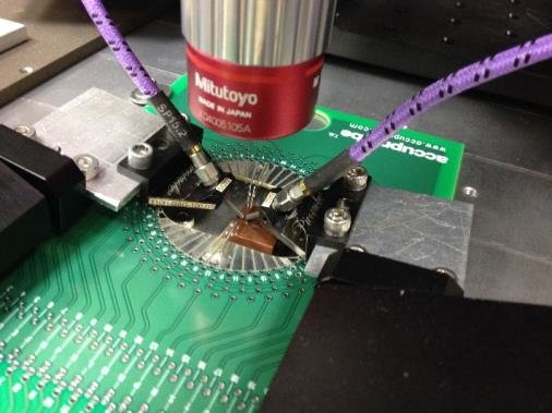
Probe card PCBs experience constant mechanical stress during probe touchdown. To maintain reliability, the PCB must offer:
-
Excellent flatness control
-
Balanced stackup design to prevent warpage
-
Reinforced structures for long-term durability
Mechanical instability directly impacts probing accuracy and test repeatability.
Materials and Stackup for Probe Card PCBs
Material selection focuses on dimensional and electrical stability:
-
High-Tg, low-CTE laminates
-
Low-loss materials for high-speed signals
-
Symmetrical multilayer stackups
These choices ensure consistent performance across temperature changes and extended test cycles.
Manufacturing Precision and Process Control
Probe card PCBs require extremely tight manufacturing tolerances:
-
Precise drilling and via registration
-
Uniform copper thickness
-
Accurate surface finish control
Any deviation can translate into misalignment or signal degradation at the probe interface.
Typical Applications of Probe Card PCBs
Probe Card PCBs are widely used in:
-
Wafer sort testing
-
Advanced logic and memory IC validation
-
Automotive and high-reliability semiconductor screening
-
RF and mixed-signal wafer-level test
Each application relies on stable probe contact and accurate signal transmission.
Choosing a Probe Card PCB Manufacturing Partner
When selecting a Probe Card PCB manufacturer, key capabilities include:
-
Experience with high pin count and HDI structures
-
Proven flatness and tolerance control
-
Strong quality management and traceability
-
Support for rapid iteration and engineering collaboration
A reliable supplier ensures consistent test performance from prototype to production.
Conclusion
The Probe Card PCB is a foundational component in wafer-level semiconductor testing. By combining mechanical precision, electrical stability, and manufacturing consistency, a well-engineered probe card PCB enables accurate measurements, higher yields, and reliable device qualification.
Partnering with an experienced Probe Card PCB supplier is essential for achieving stable, repeatable wafer probing in advanced semiconductor manufacturing.
