As data rates and operating frequencies continue to increase, signal integrity becomes a critical factor even at the prototype stage. A controlled impedance PCB prototype allows engineers to validate high-speed and RF signal performance before entering volume production.
Accurate impedance control during PCB prototyping helps reduce reflections, minimize signal loss, and ensure design reliability from the very beginning.
What Is a Controlled Impedance PCB Prototype?
A controlled impedance PCB prototype is a PCB built with precisely defined trace geometry, dielectric materials, and stackup parameters to achieve a target impedance, such as 50Ω, 90Ω, or 100Ω differential.
These prototypes are commonly used in:
-
High-speed digital designs
-
RF and microwave circuits
-
Communication and networking equipment
-
High-frequency test and measurement systems
Why Impedance Control Is Critical at the Prototype Stage
Signal Integrity Validation
Controlled impedance PCB prototypes allow early evaluation of reflections, insertion loss, and eye diagram performance.
Accurate Design Verification
Prototypes verify whether calculated impedance values match real manufacturing conditions.
Reduced Risk Before Mass Production
Early impedance validation prevents costly redesigns and delays during volume production.
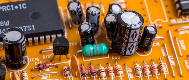
Materials Used in Controlled Impedance PCB Prototypes
Professional controlled impedance PCB prototype services support various materials, including:
-
High-Tg FR-4 for high-speed designs
-
Rogers RO4003 / RO4350 for RF circuits
-
Taconic and PTFE-based laminates
-
Hybrid stackups for cost-performance optimization
Material selection directly affects impedance stability.
Stackup Design and Impedance Calculation
Accurate controlled impedance PCB prototype manufacturing involves:
-
Detailed stackup planning
-
Impedance simulation and calculation
-
Trace width and spacing optimization
-
Dielectric thickness control
Close collaboration between design and manufacturing teams ensures accuracy.
Manufacturing Control for Impedance Accuracy
A reliable controlled impedance PCB prototype manufacturer implements:
-
Tight etching tolerance control
-
Precise lamination thickness management
-
Copper roughness optimization
-
Controlled impedance fabrication within ±5% or tighter
These processes ensure consistent prototype results.
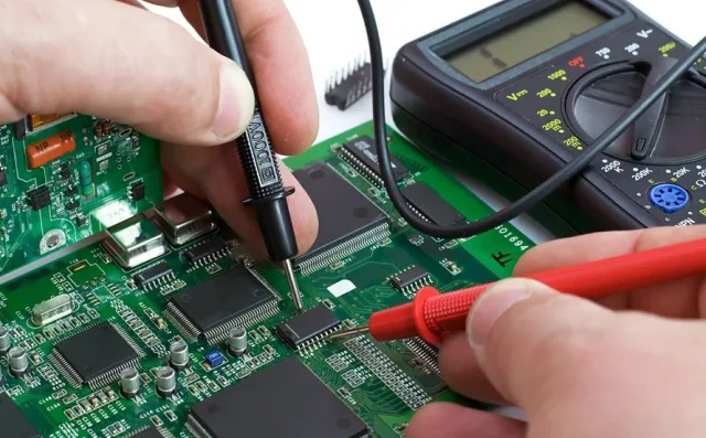
Impedance Testing and Verification
Testing is a key part of controlled impedance PCB prototype production:
-
TDR (Time Domain Reflectometry) testing
-
Impedance measurement reports
-
Electrical continuity and isolation testing
Verified impedance data provides confidence before mass production.
Rapid Turnaround for Controlled Impedance PCB Prototypes
Professional prototype services offer:
-
Quick-turn fabrication
-
Small batch production
-
Engineering feedback and DFM support
-
Seamless transition to volume manufacturing
Fast turnaround accelerates product development.
Applications of Controlled Impedance PCB Prototypes
Controlled impedance PCB prototypes are widely used in:
-
High-speed communication systems
-
RF front-end modules
-
5G and wireless devices
-
Industrial and automotive electronics
These applications demand precise impedance control and reliable signal performance.
Choosing a Supplier for Controlled Impedance PCB Prototypes
When selecting a controlled impedance PCB prototype supplier, consider:
-
Experience with high-speed and RF PCBs
-
Impedance calculation and testing capability
-
Material selection support
-
Prototype lead time and scalability
The right partner ensures accurate and reliable prototypes.
Conclusion
A controlled impedance PCB prototype is essential for validating signal integrity in high-speed and RF designs. With precise stackup design, strict manufacturing control, and verified impedance testing, controlled impedance PCB prototypes reduce development risk and accelerate time to market.
Partnering with an experienced PCB manufacturer ensures reliable controlled impedance PCB prototypes from concept to production.
