The Growing Demand for High-Frequency PCB OEM Manufacturing
With the rapid expansion of 5G/6G communication, RF modules, automotive radar, satellite systems, and high-speed networking, the demand for high-frequency PCB OEM manufacturing services has increased significantly.
Unlike standard PCB production, high-frequency PCB OEM manufacturing requires:
- Advanced RF material processing
- Precise impedance control
- Ultra-low loss design optimization
- Strict quality assurance across all production stages
From initial prototyping to full-scale production, a reliable OEM partner ensures consistent performance, fast turnaround, and scalable manufacturing capability.
At KKPCB, end-to-end solutions are provided for RF PCB development, validation, and mass production.
2. High-Frequency PCB OEM Workflow Overview
High-frequency PCB OEM manufacturing involves multiple stages:
- Design and engineering support
- Prototype fabrication
- Testing and validation
- Process optimization
- Mass production scaling
Each stage must ensure signal integrity, impedance consistency, and RF performance stability.
3. Prototype Stage: Design Validation and Rapid Iteration
3.1 Engineering Review and DFM Analysis
Before fabrication:
- Design for Manufacturability (DFM) checks
- Stack-up optimization
- Impedance simulation
Key goals:
- Identify potential risks
- Ensure manufacturability
- Optimize RF performance
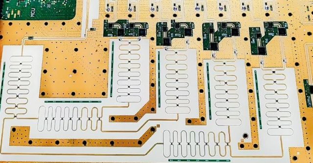
3.2 Material Selection for RF Performance
Common high-frequency materials:
- Rogers series (RO4350B, RO4835, RO3003)
- PTFE-based laminates
- Low-loss hydrocarbon materials
Critical parameters:
tanδ\tan\deltatanδ
Lower loss tangent ensures minimal signal attenuation in RF and microwave circuits.
3.3 Rapid Prototyping Capability
Prototype production focuses on:
- Fast turnaround time
- High precision fabrication
- Quick design iteration
This allows engineers to:
- Validate RF performance
- Adjust design parameters
- Reduce development cycle
4. Testing and Validation Phase
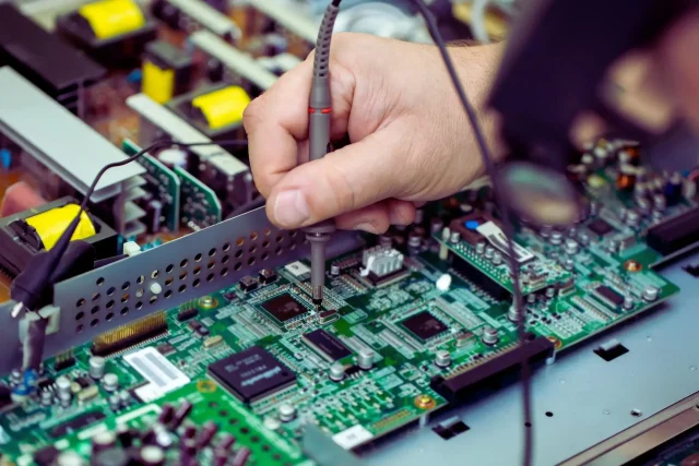
After prototyping, rigorous validation ensures performance compliance.
4.1 Electrical and RF Testing
- Impedance measurement (TDR)
- VNA testing (insertion loss, return loss)
- Signal integrity verification
4.2 Environmental Testing
- Thermal cycling
- Humidity testing
- Mechanical stress testing
4.3 Reliability Evaluation
Ensures long-term stability in:
- Automotive environments
- Aerospace systems
- Communication infrastructure
5. Process Optimization for Mass Production
5.1 Stack-Up Standardization
Standardizing stack-up ensures:
- Consistent impedance control
- Stable electrical performance
- Reduced production variability
5.2 Manufacturing Process Control
Key processes include:
- Precision lamination
- Controlled drilling and plating
- Copper roughness control
- Etching accuracy
5.3 Yield Improvement Strategies
- Process parameter optimization
- Defect reduction
- Inline inspection systems (AOI, X-ray)
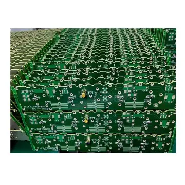
6. Mass Production: Scaling High-Frequency PCB Manufacturing
6.1 Consistency and Repeatability
Mass production requires:
- Tight process control
- Stable material supply chain
- Standardized production workflows
6.2 Quality Assurance System
Quality control includes:
- Incoming material inspection
- In-process monitoring
- Final electrical testing
6.3 Supply Chain Management
Reliable OEM manufacturing ensures:
- Stable material sourcing (Rogers/PTFE laminates)
- Short lead times
- Flexible production capacity
At KKPCB, integrated supply chain management supports efficient transition from prototype to mass production.
7. Key Challenges in High-Frequency PCB OEM Manufacturing
7.1 Material Processing Complexity
- PTFE materials are difficult to process
- Tight lamination control required
7.2 Impedance Control Requirements
Z0=LCZ_0 = \sqrt{\frac{L}{C}}Z0=CL
Maintaining consistent impedance across large volumes is critical.
7.3 RF Performance Stability
Small variations in:
- Material thickness
- Copper roughness
- Trace geometry
can significantly affect RF performance.
8. Applications of High-Frequency PCB OEM Manufacturing
High-frequency PCB OEM services are widely used in:
- 5G / 6G communication systems
- RF and microwave modules
- Automotive radar (ADAS systems)
- Satellite and aerospace communication
- High-speed networking equipment
9. KKPCB End-to-End OEM Capability
At KKPCB, services include:
- RF PCB design support and optimization
- Rapid prototyping (fast turnaround)
- Advanced RF testing (VNA, TDR)
- Mass production with strict quality control
- Full DFM and supply chain integration
This ensures:
- Seamless transition from prototype to production
- Stable RF performance
- High manufacturing yield
10. Conclusion
High-frequency PCB OEM manufacturing is a complex process that requires advanced materials, precise engineering, and strict quality control across all stages—from prototype to mass production.
By combining RF design expertise, material knowledge, and scalable manufacturing capability, companies can achieve reliable, high-performance PCB solutions for next-generation communication and electronic systems.
With proven experience and advanced capabilities, KKPCB delivers end-to-end solutions for high-frequency PCB production at scale.
