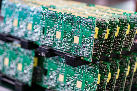
Modern industrial automation, autonomous robots, and collaborative robotic systems depend heavily on Robotics PCBs as the central electronic platform for control, sensing, and communication. Engineers designing Robotics PCBs face unique challenges: ensuring low-latency signal transmission, maintaining power stability for high-current actuators, integrating a diverse set of sensors, and protecting sensitive electronics from electromagnetic interference.
1. Signal Integrity in Robotics PCB

High-speed digital signals and precise analog sensor data require robust signal integrity. Key design strategies include:
-
Controlled impedance traces for high-speed communication
-
Differential pair routing for motor encoders, LiDAR, and camera modules
-
Short trace lengths and minimized via transitions to reduce signal reflection
-
Ground-plane optimization to provide stable return paths
Effective signal integrity design ensures robotic control systems operate reliably under real-time constraints.
2. Power Distribution and High-Current Management
Robotics PCBs must provide stable power to motors, actuators, and microcontrollers simultaneously. Engineering strategies include:
-
Wide power and ground planes to minimize voltage drop
-
Decoupling networks optimized for transient current demands
-
Separation of high-current power domains from sensitive logic or sensor circuits
-
Thermal vias and copper pours to dissipate heat efficiently
Robust power architecture improves reliability and extends the operational life of industrial and autonomous robots.
3. Sensor Integration and Interface Design

Modern robots rely on multiple sensors: LiDAR, IMUs, force sensors, joint encoders, cameras, and environmental sensors. Robotics PCB design must accommodate:
-
High-density connectors and interface pads
-
Differential signal routing for sensitive analog sensors
-
Isolation of noisy motor or power signals from sensor lines
-
Support for edge-processing modules or AI inference boards
Careful integration ensures accurate real-time perception and autonomous decision-making.
4. EMI/EMC Mitigation
Robotic environments introduce significant electromagnetic noise. Key mitigation strategies include:
-
Ground plane segmentation and stitching vias
-
Shielding of high-frequency traces
-
Filter placement at power and sensor inputs
-
Layered stackups that isolate noisy high-current traces
Proper EMI/EMC engineering maintains reliable performance even in electrically noisy industrial environments.
5. Multi-Layer Robotics PCB Stackup
Robotics PCBs often require 4–8 layer designs to balance routing complexity, signal integrity, and power delivery. Stackup considerations:
-
Dedicated ground and power planes
-
High-speed signal layers with impedance control
-
Sensor and communication layers isolated from actuator power
-
Hybrid stackups to reduce cost while maintaining performance
A well-engineered stackup is critical for high-density, high-reliability Robotics PCBs.
6. Engineering Summary
A Robotics PCB is the core of every industrial and autonomous robotic system. By optimizing signal integrity, power distribution, sensor interfaces, EMI/EMC protection, and multi-layer stackup, engineers can create robust, high-performance Robotics PCBs that enable precise control, real-time data processing, and reliable operation in complex environments.
KKPCB specializes in engineering and manufacturing Robotics PCBs that meet the demanding requirements of modern automation, collaborative robotics, and autonomous systems.

