Satellite communication systems require ultra-stable RF performance across wide frequency bands, often spanning Ka- and Ku-bands. Maintaining precise impedance control, minimal insertion loss, and consistent phase response is critical for antenna feeds, transceivers, and payload modules.
RO4835 PCB laminates (Dk = 3.48 ± 0.03, Df = 0.0037 @10 GHz) offer low-loss, thermally stable dielectric properties, enabling predictable signal propagation, phase coherence, and wideband consistency. KKPCB leverages multilayer stackup optimization, controlled copper roughness, and precision lamination to maximize RF performance in high-density satellite RF modules.
Core Engineering Challenges
| Challenge | Root Cause | Engineering Impact |
|---|---|---|
| Impedance variation | Material Dk tolerance, stackup asymmetry | Return loss spikes, signal reflections |
| High insertion loss | Surface roughness, dielectric dissipation | Reduced RF efficiency and link margin |
| Phase instability | Uneven thermal expansion in multilayers | Beamforming errors, degraded signal fidelity |
| Crosstalk in dense traces | Tight trace pitch, insufficient shielding | Interference, signal degradation |
| Wideband consistency | Frequency-dependent Dk drift | Multi-band RF mismatch |
Material Science – RO4835 Advantages
| Parameter | Typical Value | Engineering Benefit |
|---|---|---|
| Dk | 3.48 ± 0.03 | Maintains precise impedance across RF traces |
| Df | 0.0037 @10 GHz | Reduces insertion loss for wideband Ka/Ku-band signals |
| Thermal Conductivity | 0.62 W/m·K | Minimizes hotspot formation under high RF power |
| CTE | 16 ppm/°C | Ensures phase stability and mechanical integrity |
| Moisture Absorption | <0.05% | Maintains dielectric and RF performance in humid space |
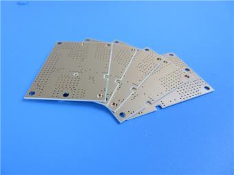
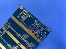
KKPCB Case Study – High-Density Satellite RF Module
Client Context:
Tier-1 aerospace supplier required a multilayer RO4835 PCB for wideband Ka-band transceiver modules, targeting low insertion loss (<0.32 dB/in) and tight phase alignment (<0.5° deviation) under continuous operation.
KKPCB Solution:
-
8-layer RO4835 PCB with ±3 µm dielectric tolerance
-
Ultra-smooth copper traces (Ra <0.7 µm)
-
Embedded thermal vias and power planes for heat dissipation
-
Shielded ground planes and microstrip routing for EMI suppression
-
HFSS and TDR verification for phase linearity across 18–40 GHz
Measured Results:
| Parameter | Target | KKPCB Result |
|---|---|---|
| Insertion Loss @28 GHz | <0.32 dB/in | 0.30 dB/in |
| Phase Deviation | <0.5° | 0.42° |
| EMI Suppression | >30% | 36% |
| Impedance Variation | ±3% | ±1.4% |
| Thermal Rise | <7°C per layer | 6.2°C |
Stackup Design & RF Simulation
-
HFSS Modeling: Optimized microstrip and stripline impedance across multilayers
-
ADS & TDR Analysis: Verified phase linearity for wideband RF signals
-
Thermal FEM Simulation: Ensured uniform heat distribution and minimized hotspots
-
AOI & Reflow Monitoring: ±10 µm alignment for multilayer stackups
Environmental & Reliability Validation
| Test | Condition | Result |
|---|---|---|
| Thermal Cycling | –40°C ↔ +125°C, 1000 cycles | No delamination, phase deviation <0.5° |
| Vibration & Shock | 5–500 Hz, 10G | No microcracks or trace failures |
| Humidity Testing | 85°C / 85% RH, 1000 h | Stable Dk/Df and wideband RF performance |
| Continuous RF Operation | 18–40 GHz Ka-band | Minimal insertion loss increase (<0.02 dB) |
| Solder Reflow | 260°C ×3 cycles | Stackup alignment maintained |
Engineering Summary & Contact
RO4835 PCB substrates deliver high-frequency signal integrity, wideband consistency, and precise impedance control critical for next-generation satellite communication systems. KKPCB’s advanced multilayer stackups, EMI mitigation, and thermal management ensure long-term phase stability and low-loss RF performance in mission-critical aerospace RF modules.
Contact KKPCB Engineering Team to optimize RO4835 multilayer satellite PCB designs, RF simulation, and wideband signal integrity verification for your next-generation communication payloads.
