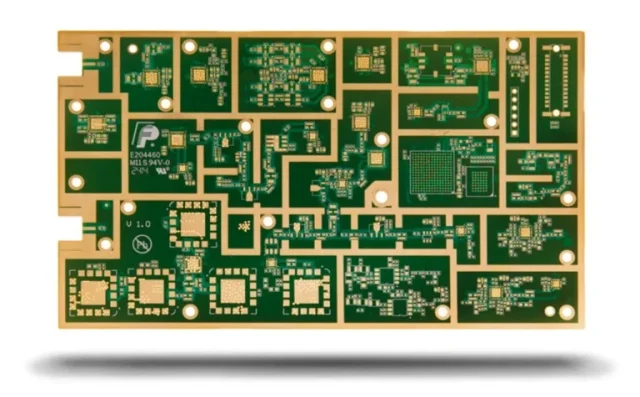
High-density RF modules used in 5G radios, SATCOM terminals, phased-array beamformers, and mmWave front-end units are increasingly constrained by thermal stress, EMI coupling, and insertion loss. As operating frequencies push beyond 10–40 GHz, traditional FR-4 structures can no longer maintain stable impedance, consistent dielectric behavior, or low-loss routing. This is where Low Loss PCB materials—such as RO4350B, RO4835, PTFE composites, and advanced hydrocarbon-ceramic laminates—become essential to preserving RF integrity.
To ensure stable RF gain, low-phase distortion, and controlled impedance in compact RF modules, KKPCB integrates engineered Low Loss PCB stackups, precision dielectric management, and EMI-suppressed multilayer routing strategies. The result is a thermally robust, low-loss interconnect platform optimized for high-frequency analog chains and dense RF architectures.
1. Thermal Performance: Core Limitation in High-Density RF Modules
As RF modules shrink and power levels rise, thermal density becomes a dominant failure mechanism. Excessive temperature increases cause:
• Dielectric constant (Dk) drift
• Higher dissipation factor (Df) and additional insertion loss
• Copper conductivity reduction
• Phase instability at mmWave frequencies
• Component aging and premature RF chain degradation
Low Loss PCB materials solve this by offering low thermal resistance, stable Dk over temperature, and high glass transition temperature (Tg).
Example performance:
| Material | Dk Stability | Thermal Conductivity | Benefit |
|---|---|---|---|
| RO4350B | ±0.05 | 0.62 W/m·K | Reduces hotspots and phase drift |
| RO4835 | ±0.03 | 0.69 W/m·K | High reliability in high-temperature RF |
| PTFE + Ceramic | Ultra-stable | 0.8–1.0 W/m·K | Extreme thermal environments |
Stable thermal performance is mandatory for PA modules、LNA front-ends、beamforming ICs、LO distribution networks operating at 28 GHz、39 GHz 和 60 GHz。
2. EMI Suppression Using Engineered Low Loss PCB Stackups
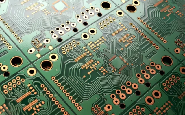
EMI propagation becomes more severe at high frequency due to shorter wavelengths and tighter module spacing. To suppress EMI, KKPCB applies:
• Segmented ground planes with stitched via fences
Reduces coupling and improves RF return pathways.
• Embedded shielding layers
Mitigates cross-domain interference between RF, digital, and power circuits.
• Low-loss dielectric separation
Minimizes field leakage and mode conversion in microstrip/stripline transitions.
• Controlled surface roughness copper
Lower roughness (Ra < 0.7 μm) maintains low-loss routing and reduces high-frequency radiation.
• Optimized stackup geometry
Symmetrical structures stabilize impedance and minimize differential skew.
These techniques allow high-density RF modules to maintain low EMI radiation, low crosstalk, and stable mmWave performance even under compact layouts.
3. Low Loss PCB Materials in RF Module Engineering
Low Loss PCB materials provide inherent benefits essential for high-density RF designs:
• Low Df ensures minimal insertion loss at mmWave
• Stable Dk improves impedance consistency
• High Tg and low CTE support thermal reliability
• Moisture resistance keeps Dk/Df stable across humidity conditions
• Better copper-dielectric bonding reduces delamination risk
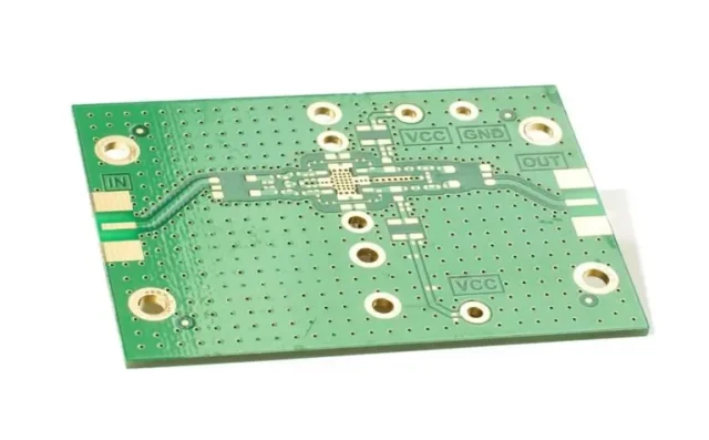
KKPCB frequently selects RO4350B, RO4835, and PTFE hybrids for:
• RF Power Amplifier Modules
• 5G FR2 Antenna-in-Package
• Beamforming Transceiver Chains
• SATCOM ODU/IDU Boards
• Millimeter-Wave Modem Cards
These materials ensure low-loss routing、high RF efficiency、low phase error、and stable thermal cycles across full operational bandwidth.
4. KKPCB Engineering Approach
To fully leverage Low Loss PCB materials, KKPCB implements:
1. Precision impedance simulation
ADS / HFSS / SIwave co-simulation ensures 50Ω / 75Ω routing accuracy.
2. Thermal finite-element modeling
Predicts junction-to-board thermal pathways for PA and LNA chains.
3. Multilayer low-loss stackups
Tightly controlled dielectric thickness improves RF phase coherence.
4. EMI / EMC shielding structures
Via fencing, cavity shielding, and embedded grounds.
5. Low-profile copper for mmWave
Reduces conductor loss at 28–60 GHz.
This engineering framework ensures that high-density RF modules maintain low insertion loss, strong EMI immunity, and robust thermal performance.
