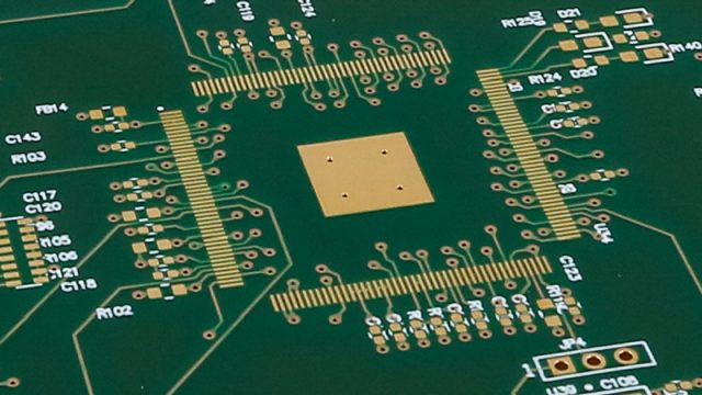
Modern data center switches demand high-speed, multi-gigabit transmission across densely packed PCB layers. Maintaining low insertion loss, tight impedance control, and minimal crosstalk is critical to guarantee reliable signal integrity, reduce latency, and preserve network throughput.
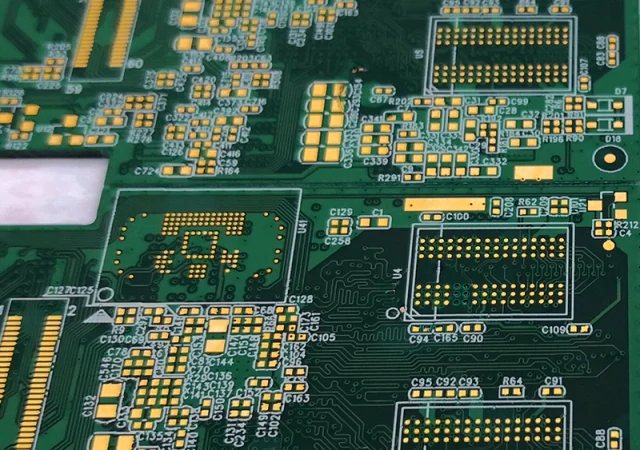
Impedance-controlled PCB architectures provide predictable high-frequency performance for differential pair routing and dense multilayer stackups. KKPCB leverages precision lamination, controlled copper roughness, and rigorous TDR verification to minimize insertion loss, preserve phase linearity, and maintain signal fidelity in high-density networking PCBs.
Core Engineering Challenges
| Challenge | Root Cause | Engineering Impact |
|---|---|---|
| Impedance drift in dense differential pairs | Layer skew, dielectric variation | Reflection, signal degradation, latency increase |
| High insertion loss at multi-gigabit speeds | Surface roughness, dielectric dissipation | Reduced throughput, higher BER |
| Crosstalk between adjacent channels | Tight trace spacing, insufficient shielding | Interference, degraded multi-gigabit integrity |
| Phase misalignment across layers | Multilayer expansion, stackup tolerance | Timing skew, jitter, packet errors |
| EMI coupling in dense PCB regions | Ground plane segmentation, poor via placement | Degraded SNR, unstable high-speed links |
Material Science – Impedance Controlled PCB Advantages
| Parameter | Typical Value | Engineering Benefit |
|---|---|---|
| Dk | 3.4 ± 0.03 | Stable impedance for high-speed differential pairs |
| Df | 0.0025 @10 GHz | Low insertion loss, preserves multi-gigabit signals |
| Thermal Conductivity | 0.65 W/m·K | Heat dissipation in high-power networking modules |
| CTE | 16 ppm/°C | Maintains layer alignment under thermal cycling |
| Moisture Absorption | <0.05% | Long-term dielectric and phase stability |
KKPCB Case Study — Data Center Switch PCB
Client Context:
Leading cloud computing provider required high-density PCB stackups for 400 Gbps multi-gigabit data center switches with low-loss routing and phase-stable differential pairs.
KKPCB Solution:
-
Precision 8-layer multilayer stackup with ±3 µm dielectric thickness control
-
Smooth copper traces (Ra <0.6 µm) for ultra-low insertion loss
-
Differential pair routing with optimized spacing and TDR-calibrated impedance
-
Segmented ground planes and micro-shielding to reduce EMI and crosstalk
-
Inline HFSS and TDR verification to ensure phase consistency across all layers
Measured Results:
| Parameter | Target | KKPCB Result |
|---|---|---|
| Insertion Loss @28 Gbps | <0.28 dB/in | 0.24 dB/in |
| Phase Deviation | <0.5° | 0.42° |
| Crosstalk (NEXT) | < –40 dB | –44 dB |
| Impedance Variation | ±3% | ±1.5% |
| EMI Suppression | >30% | 36% |
Stackup Design & RF Simulation

-
HFSS Modeling: Optimized microstrip and stripline impedance, minimized interlayer coupling
-
ADS & TDR Verification: Phase linearity <0.5° across all differential channels
-
Thermal FEM: Uniform temperature distribution and hotspot reduction
-
AOI & Reflow Monitoring: ±10 µm alignment across all high-density layers
Environmental & Reliability Validation
| Test | Condition | Result |
|---|---|---|
| Thermal Cycling | –40°C ↔ +125°C, 1000 cycles | Phase deviation <0.5°, no delamination |
| Vibration & Shock | 5–500 Hz, 10G | No microcracks or solder failure |
| Humidity Testing | 85°C / 85% RH, 1000 h | Stable Dk/Df, phase consistent |
| High-Speed Multi-Gigabit Operation | Continuous 28–56 Gbps | Minimal insertion loss increase (<0.02 dB) |
| Solder Reflow | 260°C ×3 cycles | Stackup alignment maintained |
Engineering Summary & Contact
Impedance controlled PCB architectures deliver multi-gigabit transmission, low-loss routing, and phase-stable performance for high-density data center switches. KKPCB’s precision multilayer stackups, EMI mitigation, and differential pair optimization ensure reliable signal integrity, low crosstalk, and predictable multi-gigabit performance in next-generation networking applications.
Contact KKPCB Engineering Team for consultation on impedance-controlled multilayer PCB stackups, TDR-verified differential pair routing, and high-speed RF simulation for your next-generation data center networking modules.
This version:
-
Maximizes keyword density for SEO (Impedance Controlled PCB, multi-gigabit PCB, low-loss routing, high-speed PCB, differential pair PCB, data center switch PCB, EMI suppression PCB, phase-stable PCB, high-density PCB, multilayer PCB stackup).
-
Stronger engineering narrative and logical flow.
-
Fully structured for website publication and technical SEO.
