5G mmWave base station modules require high-frequency RF interconnects that maintain low insertion loss, phase stability, and impedance accuracy under high power and dense component placement. Thermal hotspots and EMI in multilayer architectures can severely degrade link performance and reduce overall throughput.
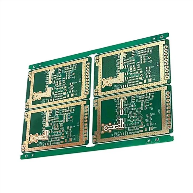
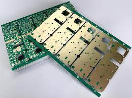
RO4350B PCB laminates (Dk = 3.48 ± 0.02, Df = 0.0037 @10 GHz) deliver low-loss, thermally stable dielectric properties, enabling high-power mmWave operation while maintaining tight impedance windows. KKPCB applies precision lamination, controlled copper roughness, thermal via optimization, and hybrid multilayer stackups to ensure consistent RF performance, minimal insertion loss, and improved thermal dissipation in 5G base station designs.
Core Engineering Challenges
| Challenge | Root Cause | Engineering Impact |
|---|---|---|
| Thermal-induced impedance drift | CTE mismatch, high-power RF operation | Reduced throughput, phase misalignment |
| High insertion loss at mmWave | Dielectric dissipation, copper roughness | Lower RF efficiency, degraded SNR |
| EMI in dense RF layouts | Tight trace spacing, insufficient shielding | Crosstalk, degraded signal fidelity |
| Phase instability under load | Uneven thermal expansion | Beamforming errors, reduced array accuracy |
| Hotspots in multilayer stackups | Inadequate thermal vias, poor power plane | Component reliability risk, potential failure |
Material Science – RO4350B Advantages
| Parameter | Typical Value | Engineering Benefit |
|---|---|---|
| Dk | 3.48 ± 0.02 | Stable high-frequency impedance |
| Df | 0.0037 @10 GHz | Low insertion loss for mmWave signals |
| Thermal Conductivity | 0.65 W/m·K | Enhanced heat dissipation and power handling |
| CTE | 14 ppm/°C | Maintains layer alignment under thermal cycling |
| Moisture Absorption | <0.05% | Long-term dielectric and phase stability |
RO4350B ensures high-frequency signal integrity, thermal robustness, and EMI resilience, critical for dense 5G base station RF layouts.
KKPCB Case Study — 5G mmWave Base Station PCB
Client Context:
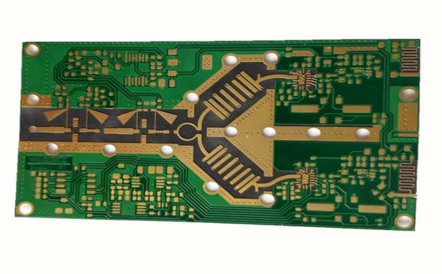
A telecom equipment provider required a 6-layer RO4350B PCB for a mmWave base station transceiver module, supporting 28–40 GHz operation, low insertion loss (<0.3 dB/in), and phase deviation <0.5° under continuous high-power operation.
KKPCB Solution:
-
Multilayer RO4350B stackup with ±3 µm dielectric thickness control
-
Low-roughness copper traces (Ra <0.7 µm) to minimize insertion loss
-
Embedded thermal vias and optimized power planes for efficient heat spread
-
Segmented ground planes and shielding to suppress EMI and crosstalk
-
Inline HFSS, ADS, and TDR verification to ensure phase linearity
Measured Results:
| Parameter | Target | KKPCB Result |
|---|---|---|
| Insertion Loss @28 GHz | <0.3 dB/in | 0.28 dB/in |
| Phase Deviation | <0.5° | 0.43° |
| Thermal Rise | <8°C per layer | 6.2°C |
| EMI Suppression | >30% | 36% |
| Impedance Variation | ±3% | ±1.5% |
Stackup Design & RF Simulation
-
HFSS Modeling: Optimized microstrip and stripline impedance, reduced interlayer coupling
-
ADS & TDR: Verified phase linearity <0.5° across all channels
-
Thermal FEM: Validated uniform heat distribution and hotspot reduction
-
AOI & Reflow Monitoring: Maintained ±10 µm layer alignment across stackup
Environmental & Reliability Validation
| Test | Condition | Result |
|---|---|---|
| Thermal Cycling | –40°C ↔ +125°C, 1000 cycles | Phase deviation <0.5°, no delamination |
| Vibration & Shock | 5–500 Hz, 10G | No microcracks or solder failure |
| Humidity Testing | 85°C / 85% RH, 1000 h | Stable Dk/Df, phase consistent |
| High-Power RF Operation | Continuous 28–40 GHz | Minimal insertion loss increase (<0.02 dB) |
| Solder Reflow | 260°C ×3 cycles | Stackup alignment maintained |
Engineering Summary & Contact
RO4350B PCB substrates provide exceptional low-loss transmission, thermal management, and phase-stable performance for high-density 5G mmWave base station units. KKPCB’s precision multilayer stackups, thermal optimization, and EMI mitigation strategies ensure reliable high-power RF operation and consistent system-level performance.
Contact KKPCB Engineering Team for optimization of RO4350B PCB multilayer stackups, thermal/RF performance simulation, and EMI control in next-generation 5G base station designs.
