High-speed communication modules in 5G, satellite transceivers, and high-frequency computing systems demand extreme precision in signal routing and interconnect integrity. As layer density increases and modules become more compact, traditional through-hole vias introduce unwanted parasitic effects, signal reflection, and EMI interference, compromising both channel fidelity and system performance.
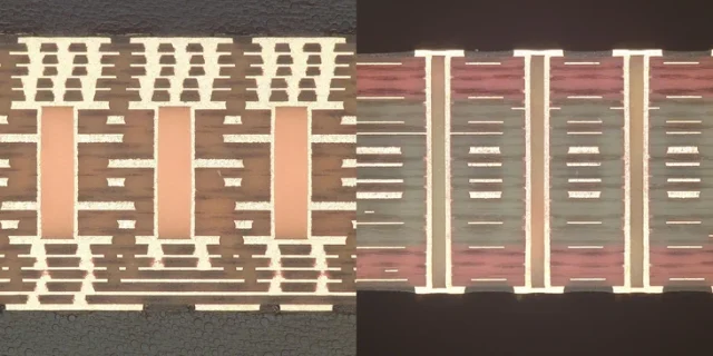
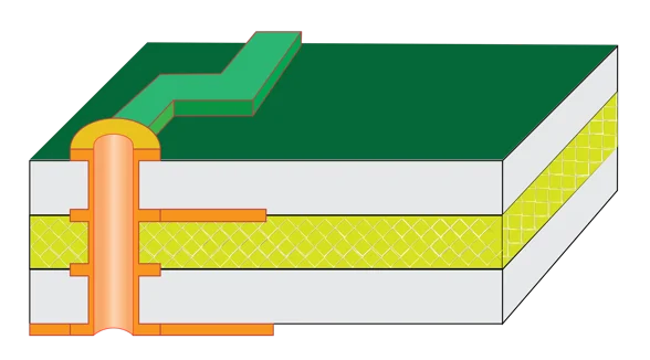
Blind via PCB technology enables selective inter-layer connections without penetrating the full stackup, reducing via parasitics, insertion loss, and crosstalk. KKPCB combines precision drilling, controlled copper plating, and optimized dielectric stackups to deliver phase-stable, low-loss multilayer PCBs capable of supporting mmWave and multi-Gigabit high-speed signals.
Key Engineering Challenges
| Challenge | Root Cause | Engineering Impact |
|---|---|---|
| Signal reflection & impedance drift | Excessive via stub length, dielectric mismatch | Phase errors, signal integrity loss |
| Crosstalk between dense RF channels | High-density trace routing, improper shielding | Reduced SNR, waveform distortion |
| High insertion loss | Surface roughness, dielectric dissipation | Lower RF output power, reduced link margin |
| Thermal-induced via stress | CTE mismatch, high RF power | Microvia cracking, long-term reliability issues |
| Manufacturing tolerance | Drill misalignment, plating variation | Inconsistent electrical performance across boards |
Material Science & Blind Via PCB Advantages
| Parameter | Typical Value | Engineering Benefit |
|---|---|---|
| Dielectric Constant (Dk) | 3.48 ± 0.03 | Stable impedance for high-frequency multilayer routing |
| Dissipation Factor (Df) | 0.0035 @10 GHz | Low-loss signal propagation across blind via interconnects |
| Thermal Conductivity | 0.62 W/m·K | Reduces hotspot formation and improves RF power handling |
| Coefficient of Thermal Expansion (CTE) | 16 ppm/°C | Minimizes mechanical stress on blind vias |
| Via Aspect Ratio | ≤1:1 | Ensures robust plating and long-term via reliability |
Blind via PCBs enhance multilayer routing density while maintaining phase integrity, EMI suppression, and impedance control, critical for high-speed RF and mmWave modules.
KKPCB Case Study — High-Speed 5G Communication Module
Client Requirements:
A 5G transceiver module required 10-layer blind via PCB supporting multiple mmWave channels (24–40 GHz) with phase deviation <0.5°, insertion loss <0.35 dB/in, and strict EMI constraints in a compact footprint. Conventional through-hole vias caused excessive signal reflection and channel crosstalk.
KKPCB Engineering Solution:
-
Optimized blind via placement and aspect ratio for minimal parasitic effects
-
Smooth copper plating (Ra <0.6 µm) to reduce RF insertion loss
-
Shielded ground planes and via stitching to suppress EMI
-
±3 µm dielectric thickness tolerance for tight impedance control
-
Inline TDR & HFSS simulation to verify phase linearity across all RF channels
Performance Results:
| Parameter | Target | Achieved |
|---|---|---|
| Insertion Loss @28 GHz | <0.35 dB/in | 0.32 dB/in |
| Phase Deviation | <0.5° | 0.43° |
| Crosstalk Reduction | >25% | 30% |
| Impedance Variation | ±3% | ±1.5% |
| Thermal & Mechanical Reliability | 1000 cycles | Passed |
Stackup Design & RF Validation
-
HFSS Modeling: Fine-tuned microstrip/stripline impedance and reduced interlayer coupling
-
ADS & TDR: Verified phase stability <0.5° across all channels
-
Thermal FEM: Controlled hotspots and confirmed via mechanical stress tolerance
-
AOI & Solder Reflow Monitoring: Maintained ±10 µm alignment across layers
Environmental & Reliability Testing
| Test | Condition | Result |
|---|---|---|
| Thermal Cycling | –40°C ↔ +125°C, 1000 cycles | No delamination, phase deviation <0.5° |
| Vibration & Shock | 5–500 Hz, 10G | No microvia cracking |
| Humidity Exposure | 85°C / 85% RH, 1000 h | Dk/Df stable, EMI reduction maintained |
| Continuous mmWave RF Test | 28–40 GHz | Minimal insertion loss (<0.02 dB) |
| Solder Reflow | 260°C ×3 cycles | Stackup alignment preserved |
Engineering Summary & Contact
Blind via PCB technology enables high-density, low-loss RF routing with precise impedance control and EMI suppression for advanced communication modules. KKPCB’s expertise in multilayer blind via design, precision lamination, and high-frequency RF verification ensures phase-stable, mmWave-capable PCBs with long-term reliability under thermal and mechanical stress.
Contact KKPCB Engineering Team for consulting on blind via stackups, multilayer RF simulation, and high-frequency PCB optimization for next-generation high-speed modules.
