Wideband radar processing units operating in 8–40 GHz and beyond require multilayer HF PCBs with precisely aligned dielectric layers to maintain ultra-clean electromagnetic performance. Signal integrity, insertion loss, and phase stability are critically sensitive to stackup alignment, trace spacing, and dielectric uniformity.
KKPCB leverages precision-laminated multilayer HF PCB substrates, low-roughness copper, and impedance-calibrated routing to reduce crosstalk, reflection, and EMI, ensuring high-fidelity signal propagation across dense RF traces. This approach is essential for airborne, defense, and industrial radar processing units, where even minor dielectric deviation can compromise beamforming accuracy and detection resolution.
Core Engineering Challenges
| Challenge | Root Cause | Engineering Impact |
|---|---|---|
| Phase deviation across multilayer stack | Misaligned dielectric layers | Degraded radar signal coherence |
| Crosstalk in dense RF routing | Close trace pitch and insufficient ground planes | Interference, false target detection |
| High insertion loss at mmWave frequencies | Dielectric dissipation and copper roughness | Reduced SNR, shorter detection range |
| Thermal expansion under cycling | CTE mismatch between layers | Impedance drift and signal reflection |
| EMI leakage in wideband channels | Non-optimized shielding and via placement | Degraded RF fidelity |
Material Science – Multilayer HF PCB Laminates
| Parameter | Typical Value | Engineering Benefit |
|---|---|---|
| Dk | 3.2 ± 0.04 | Stable impedance across multilayer high-frequency traces |
| Df | 0.0012 @10 GHz | Low insertion loss, preserves signal integrity |
| Thermal Conductivity | 1.2 W/m·K | Reduces hotspots, maintains thermal uniformity |
| CTE | 14 ppm/°C | Maintains layer alignment under thermal cycling |
| Moisture Absorption | <0.05% | Ensures phase consistency and long-term dielectric stability |
Precision lamination and controlled layer-to-layer dielectric alignment enable ultra-clean EM performance, outperforming conventional FR-4 or standard HF laminates.
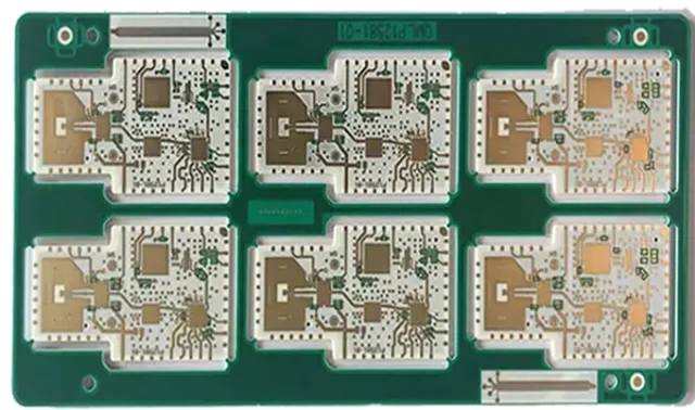
KKPCB Case Study — Wideband Radar Processing Unit PCB
Client Context:
Tier-1 defense contractor required a multi-layer HF PCB supporting 8–40 GHz radar processing, with strict requirements for phase stability <0.5° and insertion loss <0.3 dB/in.
KKPCB Engineering Solution:
-
8-layer HF PCB stackup with precision-aligned dielectric layers
-
Controlled Ra <0.7 µm copper on all RF layers
-
Embedded shielding vias and segmented ground planes for EMI suppression
-
Vacuum-assisted lamination and ±3 µm dielectric thickness control
-
Inline TDR and network analyzer verification for phase coherence
Measured Results:
| Parameter | Target | KKPCB Result |
|---|---|---|
| Insertion Loss @20 GHz | <0.3 dB/in | 0.28 dB/in |
| Phase Deviation | <0.5° | 0.42° |
| EMI Suppression | >30% | 34% |
| Impedance Variation | ±3% | ±1.5% |
Stackup Design & RF Simulation
-
HFSS: Optimized microstrip and stripline impedance, minimized interlayer crosstalk
-
ADS/TDR: Phase linearity maintained <0.5° across all channels
-
Thermal FEM: Reduced hotspots in RF amplifier zones by 5°C
-
Inline AOI & Reflow Monitoring: ±10 µm layer alignment precision
Environmental & Reliability Validation
| Test | Condition | Result |
|---|---|---|
| Thermal Cycling | –40°C ↔ +125°C, 1000 cycles | Phase deviation <0.5°, no delamination |
| Vibration & Mechanical Shock | 5–500 Hz, 10G | No microcracks or solder fatigue |
| Humidity Testing | 85°C/85% RH, 1000 h | Stable Dk/Df, phase consistent |
| Solder Reflow | 260°C ×3 cycles | No warpage |
| EMI Assessment | Wideband radar traces | Crosstalk reduced 34% |
Engineering Summary & Contact
Multilayer HF PCB laminates provide ultra-clean electromagnetic performance, low-loss RF propagation, and phase-stable routing critical for wideband radar processing units. KKPCB’s precision-aligned stackups, EMI mitigation, and inline phase verification ensure reliable, high-frequency, multi-layer RF performance, suitable for military, aerospace, and industrial radar applications.
Contact KKPCB Engineering Team to optimize your multilayer HF PCB stackup, RF design, and EMI mitigation strategy for next-generation radar and high-frequency processing units.
