Modern server motherboards require predictable impedance, extremely low jitter, and stable multi-gigabit routing to support DDR5, PCIe 6.0, and high-density network interfaces. FR-4-class materials fail to provide consistent loss and dielectric stability. Megtron 7 PCB laminates supply ultra-low Df, tight dielectric tolerances, and high-temperature reliability suited for 8–64 GT/s environments.
KKPCB adapts Megtron 7 PCB stackups for dense server motherboards where routing layers, power integrity structures, and differential pairs must coexist under strict electrical and mechanical constraints.
Engineering Challenges in High-Density Server Boards
Advanced server mainboards suffer from:
• DDR5 signal margin collapse due to inconsistent dielectric Dk
• PCIe 6.0 sensitivity to reflections and loss imbalance
• Impedance instability caused by resin-glass weave effect
• High-layer count (18–32 layer) leading to lamination stress
• Thermal hotspots deforming dielectric profiles
Megtron 7 PCB materials provide a uniform electrical platform that significantly reduces these uncertainties.
Material Science — Megtron 7 for Server Platforms
Megtron 7 PCB advantages include:
• Ultra-low Df → reduces channel attenuation for long memory runs
• Dk uniformity → tight impedance control crucial for PCIe 6.0
• High Tg and thermal durability → stable under CPU/VRM heating
• Excellent CAF resistance → safer for high-density via fields
• Low CTE → improved registration accuracy in large boards
These properties deliver consistent multi-gigabit channel behavior across the full motherboard.
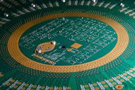
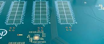
KKPCB Case Study — 28-Layer Server Board Using Megtron 7 PCB
Problem:
Customer reported DDR5 Vref instability and PCIe eye-opening collapse due to inconsistent impedance across the previous material stack.
KKPCB Megtron 7 Engineering:
• 28-layer Megtron 7 PCB stackup with balanced resin-glass distribution
• VLP copper reducing conductor-surface loss by 19%
• Tight impedance window ±6% verified by 4-port TDR
• SK-controlled memory channels with length matching <0.5 mm
• Via stub reduction through backdrill + blind/buried structure
Measured Performance:
| Parameter | Achieved |
|---|---|
| DDR5 margin | +18% improvement |
| PCIe 6.0 IL | 27% lower |
| Impedance variance | ±4.2% |
| Crosstalk | –16.7 dB |
Simulation & Stackup Engineering
• Sigrity analysis confirmed controlled glass-weave skew mitigation
• PI simulation validated VRM zones with stable impedance planes
• Thermal FEM predicted dielectric drift <0.4% around CPU hotspots
• HFSS verified differential pair consistency across all routing layers
Validation
• Power-thermal cycling (VRM region) → no delamination
• Humidity 85/85 → stable S-parameters after 500 h
• Vibration → no via-barrel cracking across dense arrays
Engineering Summary
Megtron 7 PCB stackups enable reliable, thermally stable, and electrically consistent routing for advanced server motherboards. KKPCB’s process controls ensure low-loss behavior, tight impedance tolerance, and robust long-term reliability for next-generation data-center platforms.
