Why Single Layer PCBs Still Matter
Although modern electronics are increasingly dominated by multilayer PCBs, HDI structures, and high-frequency RF boards, single layer PCBs (Single-Sided PCBs) remain widely used due to their low cost, simple design, and high manufacturability.
Single layer PCBs are still essential in:
- Cost-sensitive electronic products
- Simple analog circuits
- Power control modules
- Consumer appliances
- Educational and prototyping systems
At KKPCB, single layer PCB production is optimized for high yield, stable quality, and cost-efficient mass manufacturing.
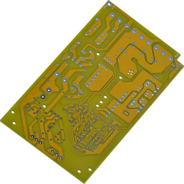
What is a Single Layer PCB? (Definition and Structure)
A single layer PCB is a printed circuit board that contains:
- Only one conductive copper layer
- Components mounted on one side only
- No internal layers or complex interconnect structures
Basic Structure:
- Component layer
- Copper conductive layer
- Insulating substrate (typically FR4, CEM-1, or phenolic resin)
- Solder mask (optional depending on design)
This simple structure makes it the most economical PCB type in the industry.
Key Design Rules for Single Layer PCBs
-
Component Placement Optimization
Since routing is limited to one side:
- Components must be arranged for minimal trace crossing
- Signal flow should follow logical sequence
- High-power components should be separated from signal circuits
-
Routing Constraints
Single layer PCBs have strict routing limitations:
- No internal layers for signal/power separation
- All traces must be routed on one copper plane
- Jumper wires may be required for complex circuits
-
Grounding Strategy
Proper grounding is critical:
- Use large ground areas where possible
- Minimize loop area to reduce noise
- Avoid long return paths
-
Thermal Considerations
Heat dissipation must be managed carefully:
- Wider traces for high-current paths
- Thermal relief pads for components
- Strategic placement of heat-generating devices
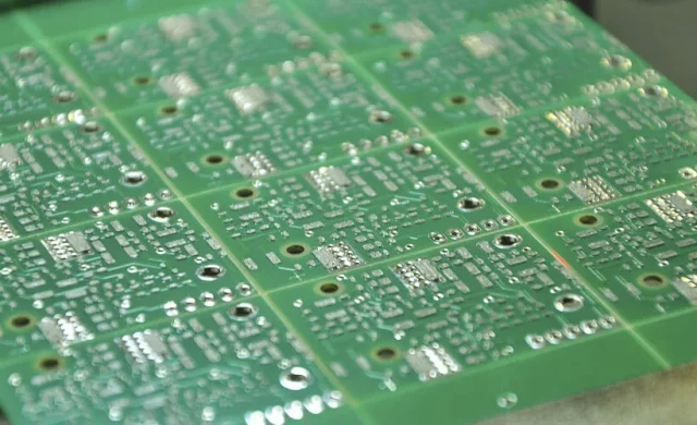
Single Layer PCB Manufacturing Process
1.1 Substrate Preparation
Common materials:
- FR4 (most widely used)
- CEM-1 / CEM-3
- Phenolic paper-based laminates (low-cost applications)
1.2 Copper Lamination
A thin copper foil is bonded to one side of the substrate using heat and pressure.
1.3 Circuit Pattern Printing
- Photoresist coating
- UV exposure through artwork film
- Development process to define circuit pattern
1.4 Etching Process
Unwanted copper is removed using chemical etching, leaving only the designed circuit traces.
1.5 Drilling Process
Holes are drilled for:
- Component leads
- Mechanical mounting
Since there are no vias between layers, drilling is simpler than multilayer PCBs.
1.6 Surface Finishing
Depending on application:
- HASL (Hot Air Solder Leveling)
- OSP (Organic Solderability Preservative)
- ENIG (for higher reliability designs)
1.7 Solder Mask and Silkscreen
- Solder mask protects copper traces
- Silkscreen provides component labeling
Advantages of Single Layer PCBs
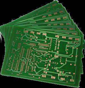
1. Low Cost Manufacturing
- Simplest PCB structure
- Minimal processing steps
- Ideal for mass production
2. Easy Design and Debugging
- Simple layout
- Easy troubleshooting
- Fast prototyping
3. High Reliability for Simple Circuits
- Fewer interconnections
- Lower failure probability
- Strong mechanical stability
4. Fast Production Cycle
- Short manufacturing lead time
- Efficient fabrication process
Limitations of Single Layer PCBs
Limited Circuit Complexity
- Not suitable for high-density designs
- Limited routing space
Larger Board Size
- Requires more physical space for routing
- Less suitable for miniaturized devices
Poor High-Speed Performance
- No controlled impedance capability
- Higher EMI susceptibility
- Not suitable for RF or high-frequency circuits
Applications of Single Layer PCBs
Single layer PCBs are widely used in:
Consumer Electronics
- Radios
- Calculators
- LED lighting systems
Power Electronics
- Power adapters
- Simple converters
- Battery chargers
Industrial Equipment
- Control panels
- Relay boards
- Basic automation systems
Educational and Prototyping Use
- Training kits
- Hobby electronics
Single Layer PCB vs Multilayer PCB
| Feature | Single Layer PCB | Multilayer PCB |
|---|---|---|
| Cost | Low | High |
| Complexity | Low | High |
| Routing | Limited | Advanced |
| Size | Larger | Compact |
| Performance | Basic | High-speed & RF capable |
KKPCB Single Layer PCB Manufacturing Capability
At KKPCB, single layer PCB production includes:
- High-volume mass production capability
- Strict quality control (AOI inspection)
- Stable copper etching precision
- Reliable solderability testing
- Cost-optimized manufacturing processes
This ensures consistent quality and high production efficiency for industrial-scale applications.
Conclusion
Single layer PCBs remain a fundamental and highly cost-effective solution in electronics manufacturing. While they are limited in complexity and high-speed performance, they offer excellent value for simple, low-cost, and reliable electronic designs.
With advanced manufacturing capabilities and strict process control, KKPCB provides stable and efficient single layer PCB solutions for global electronics industries.
