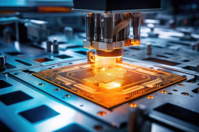
In the semiconductor manufacturing process, wafer testing is a critical step to ensure device functionality, performance, and yield before packaging. Wafer Test PCBs are specialized printed circuit boards that interface directly with wafer probe cards and automated test equipment (ATE), providing reliable signal routing, controlled impedance, and mechanical stability across thousands of test cycles.
By enabling precise and repeatable testing, wafer test PCBs play a pivotal role in semiconductor quality control.
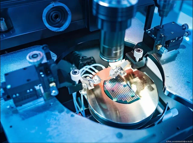
What Is a Wafer Test PCB?
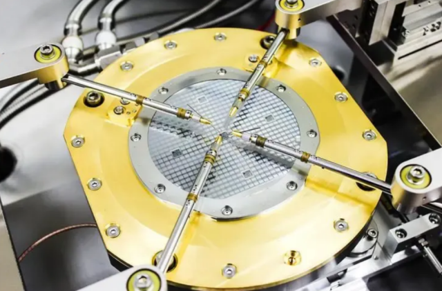
A wafer test PCB serves as the connection between the wafer under test and the ATE system. Its key functions include:
-
High-density routing for wafer-level ICs
-
Stable and low-noise power delivery
-
Controlled impedance for high-speed and RF signals
-
Mechanical alignment and reliability with probe cards
This ensures accurate electrical measurement and reduces the risk of false failures.
Key Features of Wafer Test PCBs
High-quality wafer test PCBs are designed with:
-
Controlled Impedance Routing: Minimizes reflections and preserves signal integrity at high frequencies.
-
Multilayer Stackups: Supports dense interconnects for high pin count ICs and multiple power/ground planes.
-
Mechanical Precision: Maintains probe alignment and withstands repeated test cycles.
-
Thermal Management: Effectively dissipates heat to prevent performance degradation during extended testing.
These features guarantee consistent and repeatable semiconductor testing results.
Material Selection and Stackup Design
Material choice directly impacts electrical and mechanical performance. Wafer test PCBs often use:
-
High-Tg FR-4 for standard test boards
-
Low-loss laminates for high-frequency or RF ICs
-
Hybrid stackups to balance cost and signal performance
Proper stackup design ensures reliable impedance control, minimal signal loss, and long-term durability.
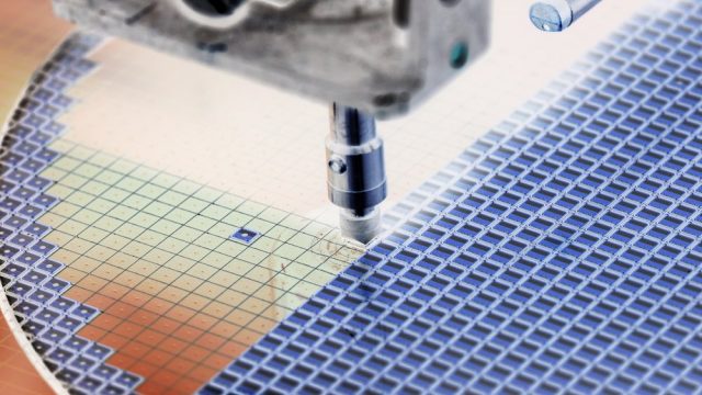
Applications of Wafer Test PCBs
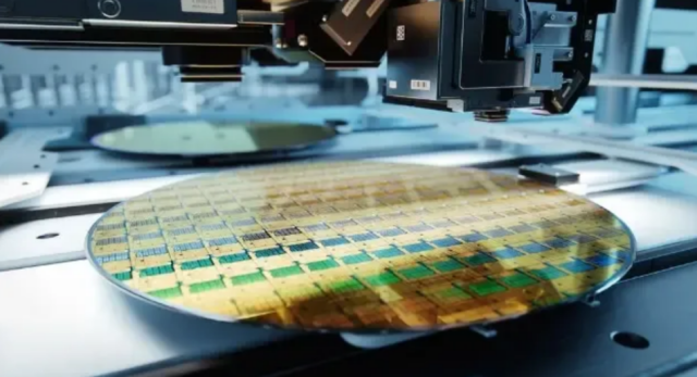
Wafer test PCBs are essential in:
-
Wafer-level functional and parametric testing
-
IC characterization and burn-in testing
-
High-density probe card interfaces for ATE
-
High-speed, mixed-signal, and RF testing
These boards are critical for ensuring accurate IC validation prior to final packaging.
Choosing a Wafer Test PCB Manufacturer
When selecting a wafer test PCB supplier, look for:
-
Experience with high pin count and high-speed wafer-level designs
-
Capability for multilayer and controlled impedance PCBs
-
Support for prototype, small batch, and volume production
-
Strong quality control and electrical verification procedures
A professional manufacturer ensures precise, repeatable, and reliable wafer testing.
Conclusion
Wafer Test PCBs are the backbone of semiconductor wafer validation, delivering controlled impedance, high-density routing, and mechanical reliability. By providing accurate and repeatable testing, these PCBs improve IC yield and overall manufacturing quality.
Partnering with a trusted wafer test PCB manufacturer ensures high-performance, reliable, and scalable solutions from prototype to production.
