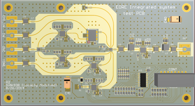
In high-speed and high-frequency electronic applications, RF PCB stack-up design plays a decisive role in ensuring stable performance, minimal signal loss, and electromagnetic compatibility. Proper PCB layer stack-up is not just a structural consideration—it directly determines signal integrity, impedance control, and overall product reliability.
This article reveals the core principles of RF PCB stacking, explains the key components of a high-frequency PCB, and provides effective optimization strategies to improve RF performance and reduce EMI.
What Is RF PCB Stack-Up Design?
RF PCB stack-up refers to a design approach where multiple PCB layers are strategically stacked to optimize electrical performance and enable high-frequency circuit functionality. Through precise stacking, designers can:
-
Increase circuit density in compact spaces,
-
Improve signal isolation and ground return paths,
-
Achieve superior electromagnetic compatibility (EMC).
In modern RF systems—such as wireless communication devices, radar modules, and high-speed network equipment—a well-designed stack-up is the foundation for low-loss signal transmission and high power efficiency.
Key Components of a High-Frequency PCB Stack-Up
1. Signal Layers
Signal layers carry RF and high-speed digital signals. Their layout must maintain consistent impedance and short signal paths to prevent reflection and attenuation.
Optimization Tip: Keep RF traces on the outer layer adjacent to a continuous ground plane for the shortest and cleanest signal return path.
2. Ground Layers
Ground planes are essential for signal stability and EMI suppression. A continuous ground plane minimizes noise coupling between layers and provides a solid reference for impedance control.
Best Practice: Place a ground plane directly beneath the RF signal layer (typically on the second layer) to ensure effective shielding and stable impedance.
3. Power Layers
Power layers supply stable voltage to circuits and must be well-positioned relative to signal layers to maintain power integrity (PI). The spacing between power and ground planes acts as a decoupling capacitor, improving high-frequency noise suppression.
4. Insulating (Dielectric) Layers
Dielectric layers separate signal and power layers, preventing interference. The dielectric constant (Dk) and dissipation factor (Df) of the material determine signal speed and loss.
Recommended Materials: Use low-Dk, low-loss laminates such as Rogers, Taconic, or Isola for high-frequency applications.

5. Vias
Vias connect different layers in a multi-layer PCB. However, excessive vias introduce signal reflection and insertion loss.
Design Rule: Minimize via transitions in RF paths and use blind or buried vias if necessary to reduce discontinuities.
Design Principles for RF PCB Stack-Up
To achieve optimal performance in high-frequency PCB design, the following principles must be observed:
-
Ground Management: Place the main ground plane on Layer 2 to provide an effective return path for RF signals on the top layer.
-
Signal and Power Layer Layout: Maintain symmetry in layer distribution for consistent impedance and minimal signal distortion.
-
Via Optimization: Reduce the number and diameter of vias to lower parasitic effects and improve signal transmission efficiency.
-
Controlled Impedance: Use impedance-controlled routing (e.g., 50Ω microstrip or 100Ω differential pair) throughout the design.
Critical Considerations in High-Frequency PCB Design
-
Impedance Matching:
The signal trace width and dielectric spacing must be carefully calculated to achieve target impedance and minimize signal reflection. -
Thermal Management:
RF circuits often generate significant heat. A balanced stack-up structure with thermal vias and copper pours helps maintain temperature stability. -
EMI Suppression:
Proper grounding, shielding, and layer arrangement can drastically reduce electromagnetic interference and improve signal-to-noise ratio (SNR).
Six Proven Strategies to Optimize RF PCB Stack-Up Design
1. Optimize Layer Configuration
Design a balanced layer stack-up with proper spacing between signal and ground layers. This minimizes cross-talk and enhances signal integrity.
2. Select High-Performance Materials
Choose low-loss dielectric materials (low Dk, low Df) to ensure faster signal transmission and reduced distortion in high-frequency circuits.
3. Shorten Trace Lengths
Keep RF signal paths as short and straight as possible. Avoid unnecessary bends, vias, and stubs to reduce propagation delay and phase noise.
4. Implement Multiple Ground Planes
Using multiple ground planes enhances return current paths, reduces EMI, and strengthens the power distribution network (PDN).
5. Apply Accurate Impedance Matching
Design traces with precise width and spacing to achieve consistent impedance. Use simulation tools (like HFSS or ADS) for pre-layout verification.
6. Follow Advanced Routing Strategies
Maintain adequate spacing between differential pairs, use matched terminations, and apply proper reference plane changes to ensure high-speed signal performance.
Why RF PCB Stack-Up Design Matters
In the realm of high-frequency PCB design, stack-up configuration determines far more than physical structure—it defines signal behavior, EMI resilience, and overall system performance.
By integrating proper ground management, low-loss materials, and optimized impedance control, engineers can create RF PCBs with superior reliability, low signal loss, and outstanding frequency response.
A well-executed RF PCB stack-up is not just good design—it’s the foundation of every high-performance electronic product.

