
With the increasing complexity of modern electronic products, traditional single-layer and double-layer PCBs can no longer meet the requirements of high-density circuits, high-speed signals, and advanced functionality.
Multi-layer PCB technology has become an essential solution for applications requiring:
- Higher circuit density
- More complex signal routing
- Improved electrical performance
- Better space utilization
- Enhanced product reliability
However, manufacturing multi-layer PCBs is significantly more challenging than producing standard PCBs. The increased number of layers introduces greater complexity in material selection, lamination, signal integrity control, and manufacturing processes.
This article explores the major challenges involved in multi-layer PCB manufacturing and how advanced PCB manufacturing techniques help overcome these difficulties.
What Is a Multi-Layer PCB?
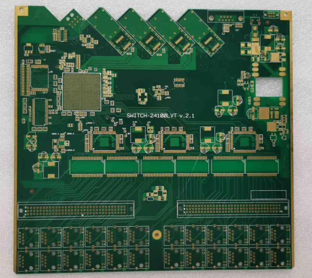
A multi-layer PCB is a printed circuit board consisting of three or more conductive copper layers separated by insulating dielectric materials.
Unlike single-layer or double-layer PCBs, multi-layer boards contain:
- Multiple signal layers
- Internal power and ground planes
- Prepreg and core materials
- Complex via structures
Typical multi-layer PCB structures include:
- 4-layer PCB
- 6-layer PCB
- 8-layer PCB
- 10+ layer high-layer-count PCB
They are widely used in:
- Industrial control systems
- Communication equipment
- Automotive electronics
- Medical devices
- Semiconductor test equipment
- High-performance computing systems
Major Challenges in Multi-Layer PCB Manufacturing
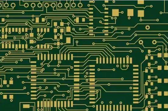
1. Complex Layer Stack-Up Design
One of the biggest challenges in multi-layer PCB manufacturing is creating a proper layer stack-up.
A multi-layer PCB must balance:
- Signal routing requirements
- Power distribution
- Grounding performance
- Mechanical stability
- Manufacturing feasibility
Poor stack-up design can result in:
- Signal interference
- Increased electromagnetic radiation
- Impedance variation
- PCB warpage
Engineers need to carefully define:
- Copper thickness
- Dielectric thickness
- Material selection
- Layer arrangement
A symmetrical stack-up design is often required to reduce mechanical stress and improve reliability.
2. Signal Integrity Control
As PCB operating frequencies increase, signal integrity becomes a major concern.
High-speed signals traveling through multiple layers may experience:
- Signal loss
- Crosstalk
- Reflection
- Impedance mismatch
Factors affecting signal performance include:
- Trace geometry
- Dielectric constant
- Routing distance
- Via structures
- Return path design
To maintain signal integrity, engineers must optimize:
- Controlled impedance routing
- Differential pair design
- High-speed signal layer allocation
- Ground plane continuity
This is especially critical for applications involving:
- High-speed communication
- RF circuits
- Memory interfaces
- Semiconductor testing systems
3. Lamination Process Control
The lamination process is one of the most critical steps in multi-layer PCB manufacturing.
During lamination:
are pressed together under controlled:
- Temperature
- Pressure
- Time
Manufacturing challenges include:
Layer Misalignment
Even small alignment errors can affect:
- Via connections
- Fine-pitch routing
- Electrical performance
Resin Flow Control
Incorrect resin flow may cause:
- Voids
- Uneven dielectric thickness
- Reliability problems
Thermal Stress
Repeated heating cycles may cause:
- Layer deformation
- PCB warpage
- Internal stress
Precise process control is essential to achieve stable multi-layer structures.
4. Via Manufacturing Challenges
Vias provide electrical connections between different PCB layers.
However, as PCB designs become more complex, via structures become increasingly difficult to manufacture.
Common challenges include:
Through-Hole Vias
Challenges:
- Higher aspect ratio
- Copper plating difficulty
- Signal loss at high frequencies
Blind and Buried Vias
Advantages:
- Save PCB space
- Improve routing density
Challenges:
- Higher manufacturing complexity
- More strict process control
- Higher production cost
Microvias
Used in HDI PCB technology, microvias require:
- Laser drilling
- Precise copper plating
- Advanced inspection methods
Poor via quality may cause:
- Open circuits
- Reliability failures
- Intermittent connections
5. Material Selection Difficulties
Different applications require different PCB materials.
Material selection affects:
- Signal performance
- Thermal behavior
- Mechanical reliability
- Manufacturing cost
Common materials include:
FR-4
Suitable for:
- General electronics
- Industrial applications
Advantages:
- Cost-effective
- Reliable performance
High-TG Materials
Used for:
- High-temperature applications
- Automotive electronics
- Industrial systems
Advantages:
- Better thermal stability
- Reduced deformation
High-Frequency Materials
Used for:
- RF systems
- Microwave applications
- High-speed communication
Advantages:
- Low dielectric loss
- Stable electrical performance
Choosing the wrong material may result in:
- Signal degradation
- Thermal problems
- Reduced product lifetime
6. PCB Warpage Control
As layer counts increase, controlling PCB flatness becomes more difficult.
Multi-layer PCB warpage can be caused by:
- Uneven copper distribution
- Asymmetrical layer design
- Thermal expansion differences
- Lamination stress
Warpage may lead to:
- SMT assembly problems
- Component misalignment
- Poor solder joints
Manufacturers must optimize:
- Stack-up symmetry
- Material balance
- Lamination parameters
- Cooling processes
7. Manufacturing Yield and Inspection Challenges
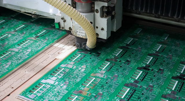
Higher layer counts increase the possibility of manufacturing defects.
Potential defects include:
- Internal layer open circuits
- Short circuits
- Lamination voids
- Copper thickness variation
- Via defects
Advanced inspection methods are required, including:
Automated Optical Inspection (AOI)
Used for:
- Inner layer inspection
- Pattern verification
X-Ray Inspection
Used for:
- Hidden structures
- Via quality
- Internal defects
Electrical Testing
Used for:
- Continuity testing
- Isolation testing
Strict quality control helps ensure multi-layer PCB reliability.
How PCB Manufacturers Overcome Multi-Layer PCB Challenges
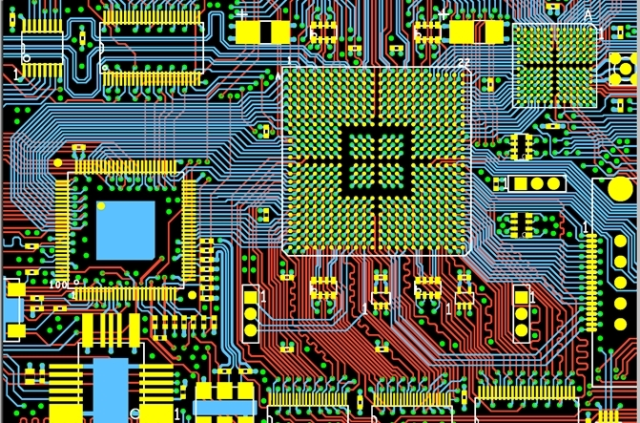
Professional PCB manufacturers use engineering expertise and advanced processes to improve production success.
Key approaches include:
Advanced Engineering Review
Including:
- Stack-up optimization
- Signal integrity analysis
- DFM evaluation
- Manufacturability assessment
Precision Manufacturing
Using:
- Laser drilling
- Controlled lamination
- High-accuracy imaging
- Advanced plating technology
Comprehensive Testing
Including:
- AOI inspection
- Flying probe testing
- Electrical testing
- Reliability verification
Applications Requiring Advanced Multi-Layer PCBs
Multi-layer PCBs are widely used in industries where reliability and performance are critical.
Examples include:
Industrial Automation
Used for:
- Control systems
- Motion controllers
- Industrial communication equipment
Automotive Electronics
Used for:
- Battery management systems
- ADAS electronics
- Vehicle control modules
Semiconductor Equipment
Used for:
- ATE load boards
- Test interfaces
- High-speed measurement systems
Communication Systems
Used for:
- RF equipment
- Network devices
- High-frequency applications
Conclusion
Manufacturing multi-layer PCB circuit boards requires advanced engineering knowledge, precise process control, and strict quality management.
The major challenges include:
- Complex stack-up design
- Signal integrity control
- Lamination accuracy
- Via reliability
- Material selection
- Warpage prevention
- Manufacturing inspection
As electronic products continue moving toward higher integration and faster performance, multi-layer PCB technology will remain a key foundation for advanced electronic systems.
By combining optimized PCB design, precision manufacturing processes, and comprehensive testing, experienced PCB manufacturers can help customers achieve reliable, high-performance multi-layer PCB solutions.
