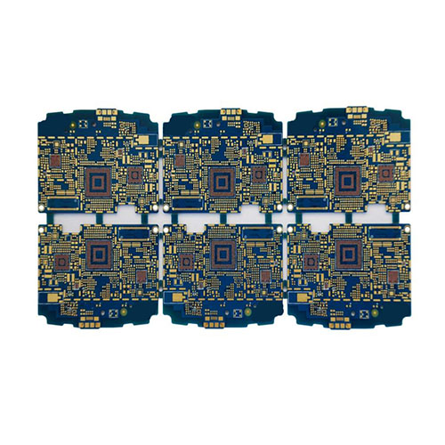
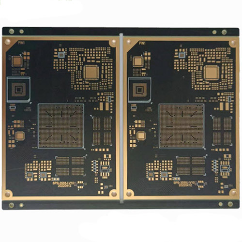
As modern electronics evolve toward smaller, faster, and more powerful systems, High-Density Interconnect (HDI) PCB technology has become the backbone of next-generation product design.
As a professional one-stop PCB and PCBA solution provider, KKPCB is committed to delivering high-performance HDI printed circuit boards that meet the increasing demands for miniaturization, precision, and reliability in today’s electronics industry.
What Is an HDI PCB?
An HDI PCB (High-Density Interconnect) is a printed circuit board that offers a significantly higher wiring density per unit area than standard PCBs.
Key technical features include microvia technology, blind and buried vias, multi-layer build-up laminations, and superior signal integrity.
As electronic devices continue to shrink in size while increasing in functionality, traditional PCB structures are no longer sufficient for high-speed data transmission and complex integration.
HDI technology enables finer lines, smaller vias and pads, and denser interconnects — resulting in lighter, thinner, and higher-performance circuit boards capable of replacing multiple standard PCBs with a single compact design.
Technical Advantages of HDI PCBs
1. Superior Signal Integrity
Microvias and short interconnection paths greatly reduce signal delay and interference, ensuring stable high-speed transmission — a critical factor for 5G, AI computing, and data communication systems.
2. Compact and Lightweight Design
HDI technology allows for reduced layer counts and optimized component layout, achieving smaller and lighter boards without compromising functionality.
Ideal for smartphones, wearables, UAVs, and portable medical electronics.
3. High Reliability and Thermal Stability
Microvia structures feature lower aspect ratios, which increase mechanical strength and improve via reliability.
High-quality build-up materials ensure electrical stability under demanding thermal and mechanical stress.
4. Flexible Design and Cost Optimization
By integrating complex functionality into fewer layers, HDI PCBs reduce material usage, simplify assembly, and shorten product development cycles — achieving a balance between performance and production efficiency.
HDI PCB Structural Types
HDI PCB (1+N+1): The Basic HDI Structure
The simplest HDI configuration includes one high-density build-up layer, ideal for BGA packages with lower I/O counts.
It provides stable mounting, precise registration, and excellent reliability.
Applications: Smartphones, GPS modules, MP3 players, memory cards.
HDI PCB (2+N+2): Moderate Complexity
This configuration features two or more build-up layers with staggered or stacked microvias.
It enables high routing density while maintaining thin board profiles and superior electrical performance.
Applications: Tablets, PDAs, handheld game consoles, video devices.
ELIC (Every Layer Interconnection): The Most Advanced HDI Structure
In ELIC designs, every layer is a high-density interconnect layer, allowing full interconnection between all layers through copper-filled stacked microvias.
It offers unmatched electrical characteristics and is ideal for CPU/GPU modules, servers, and ultra-mobile computing devices.
Applications: Smartphones, mini PCs, advanced memory modules, and high-performance computing systems.
Common Applications of HDI PCBs
HDI PCBs are widely adopted across industries requiring compact design and high-speed signal performance:
-
Consumer Electronics: Smartphones, laptops, wearables
-
Telecommunications: 4G/5G modules, RF/microwave equipment, base stations
-
Automotive Electronics: ADAS, radar systems, sensor controllers
-
Medical Devices: Monitoring instruments, imaging systems, surgical navigation
-
Aerospace and Defense: Navigation systems, avionics, guided weaponry
-
Industrial IoT and Automation: Smart sensors, control modules, robotics
KKPCB’s HDI Manufacturing Capability
KKPCB offers comprehensive engineering and manufacturing solutions for HDI PCB production — from conceptual design, material selection, and layer stackup planning to precision fabrication and mass production.
Our HDI PCB capabilities include:
-
Layer Count: Up to 36 layers
-
Copper Thickness: Up to 20 oz
-
Laser Drilling Accuracy: ±20 μm
-
Minimum Trace/Space: 50 μm / 50 μm
-
Prototype Lead Time: As fast as 48 hours
Through advanced equipment, strict quality management, and decades of technical expertise, KKPCB ensures that every HDI PCB we produce delivers outstanding electrical performance, long-term reliability, and superior cost-efficiency.
KKPCB continues to partner with global innovators to support high-speed, high-density, and high-reliability electronics — empowering the technologies shaping the future of connectivity and intelligent design.
