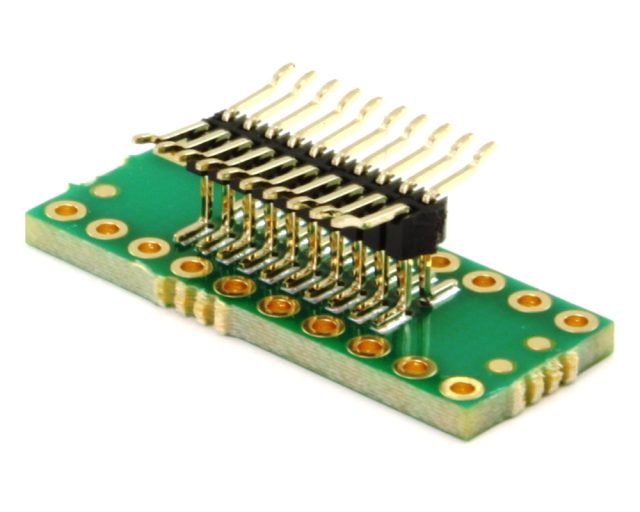
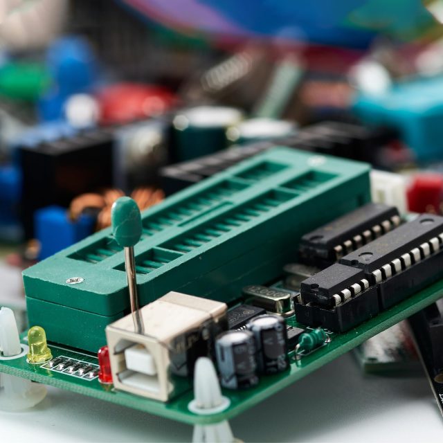
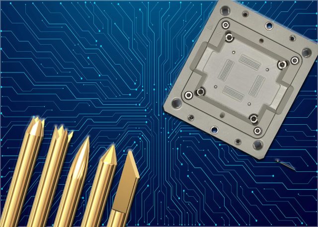
In semiconductor testing, consistent electrical contact is essential for accurate and repeatable results. The Test Socket PCB serves as the mechanical and electrical foundation that supports test sockets, ensuring stable signal transmission between the device under test and the test system.
A professionally engineered test socket PCB is critical for maintaining test accuracy throughout high-cycle testing operations.
What Is a Test Socket PCB?
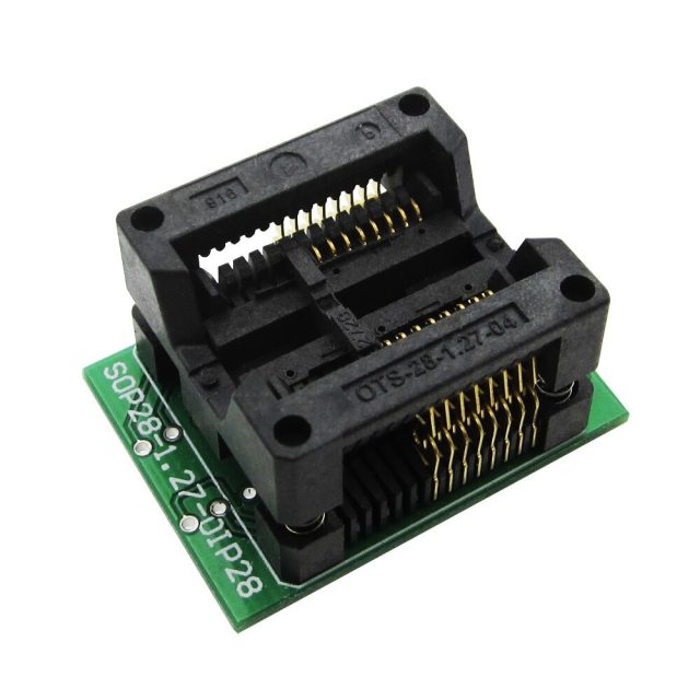
A Test Socket PCB is a specialized printed circuit board designed to:
-
Mount and support semiconductor test sockets
-
Route signals between the device and test equipment
-
Maintain precise mechanical alignment
It is commonly used in package-level and production testing environments.
Why Test Socket PCBs Are Critical
Test socket PCBs operate under demanding conditions, including:
-
Frequent device insertion and removal
-
Mechanical stress from contact force
-
Long-duration test cycles
A robust test socket PCB prevents intermittent contact and false test failures.
Signal Integrity Considerations
Even short interconnects can affect signal quality. Test socket PCBs are designed to:
-
Maintain controlled impedance
-
Minimize signal path discontinuities
-
Reduce crosstalk and noise
Good signal integrity ensures accurate pass/fail decisions.
Mechanical Strength and Flatness Control
Mechanical reliability is a key requirement. Test socket PCBs focus on:
-
Controlled board thickness and rigidity
-
Tight flatness tolerances
-
Reinforced mounting areas around sockets
Stable mechanics ensure consistent contact pressure across all pins.
High Pin Count and Dense Routing Support
Modern devices often require:
-
High pin count socket interfaces
-
Dense signal breakout
-
Multilayer routing with reference planes
Advanced PCB stackups support these needs without compromising reliability.
Material Selection and Stackup Design
Typical materials include:
-
High-Tg FR-4 for mechanical durability
-
Low-loss laminates for high-speed signals
-
Hybrid stackups for performance optimization
Material stability supports repeatable test conditions.
Manufacturing Precision and Quality Control
Manufacturing a test socket PCB requires:
-
Accurate drilling and layer registration
-
Strong via plating for mechanical stress resistance
-
Electrical continuity and impedance testing
Strict quality control ensures long-term consistency.
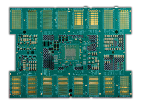
Typical Applications of Test Socket PCBs
Test socket PCBs are widely used in:
-
Semiconductor package-level testing
-
Production screening and final test
-
Reliability and life-cycle testing
-
Device characterization platforms
Each application demands stable electrical and mechanical performance.
Choosing a Test Socket PCB Manufacturer
When selecting a test socket PCB supplier, consider:
-
Experience with semiconductor test boards
-
Capability for high pin count and multilayer designs
-
Mechanical reliability and flatness control
-
Support from prototype to volume production
A trusted partner reduces test downtime and yield loss.
Conclusion
The Test Socket PCB is a critical interface component in semiconductor testing. By combining controlled impedance design, mechanical robustness, and precise manufacturing, test socket PCBs ensure accurate and repeatable test results across high-cycle test environments.
Partnering with an experienced test socket PCB manufacturer ensures stable performance throughout the entire testing lifecycle.
