Silicon Carbide (SiC) PCB technology is transforming the landscape of high-power, high-frequency, and high-temperature electronics. As electric vehicles, renewable energy converters, aerospace systems, and industrial automation demand greater efficiency and reliability, SiC PCBs provide the thermal conductivity, voltage endurance, and switching performance required for next-generation power platforms.
Unlike traditional FR-4 or low-temperature laminates, SiC PCB substrates and hybrid SiC-based stackups deliver superior thermal dissipation, electrical insulation strength, and mechanical stability—making them ideal for wide-bandgap semiconductor modules.
1. Material Science Foundation of SiC PCB

SiC PCBs leverage the unique properties of Silicon Carbide substrates or SiC-reinforced ceramic boards:
-
Thermal Conductivity: 250–320 W/m·K — enabling extreme heat dissipation
-
Wide Bandgap (3.2 eV) — supporting high-temperature, high-voltage operation
-
Dielectric Strength > 10 kV/mm — suitable for high-isolation power converters
-
Low Leakage Current & High Breakdown Voltage
-
Low CTE (~4.3 ppm/°C) — reducing thermal-mechanical stress
These material advantages enable SiC PCB structures to outperform standard ceramic or aluminum-based power substrates in harsh operating environments.
2. Thermal Management Strategies for SiC PCB
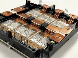
The primary advantage of SiC PCB lies in its ability to sustain and dissipate extreme heat generated by SiC MOSFETs and SiC power modules. Key engineering techniques include:
-
Direct Bonded Copper (DBC) on SiC for maximum heat conduction
-
Heavy copper planes (2–12 oz) to handle high current
-
Thermal vias beneath MOSFET/IGBT pads
-
Sintered silver die-attach for high-temperature junctions
-
Integrated heat-spreading ceramic cores
These thermal measures ensure stability in EV traction inverters, industrial power drives, and aerospace power systems.
3. High-Voltage and High-Current Layout Engineering
A SiC PCB must support extremely high voltages and currents common in wide-bandgap power systems:
-
Creepage & clearance optimization for 600V–1700V systems
-
Arc-prevention design with enlarged isolation distances
-
Copper thickness calculations for continuous high-current conduction
-
Kelvin-source routing for SiC MOSFET gate stability
-
Low-inductance busbar-style PCB structures
These engineering techniques minimize switching noise and prevent breakdown under high-voltage stress.
4. High-Frequency Switching Performance
SiC MOSFETs enable switching frequencies 3–10× higher than silicon devices. To support this, a SiC PCB requires:
-
Short, wide traces for ultra-low inductance
-
Controlled impedance for gate driver signals
-
Partitioned power-loop layout to minimize ringing
-
EMI-optimized stackup for fast dv/dt transitions
-
Shielded gate-driver sections for noise immunity
High-frequency optimization ensures clean switching, reduced losses, and stable gate behavior.
5. SiC PCB Stackup and Metallization Options
Common SiC PCB configurations include:
-
DBC SiC (Direct Bonded Copper on SiC)
-
AMB SiC (Active Metal Brazed SiC)
-
SiC-AlN Hybrid Stackup
-
SiC Metal-Core PCB (MCPCB)
-
SiC Ceramic Multilayer PCB
Metallization choices:
-
Copper — high current capacity
-
Silver (Ag) — for high-temperature conduction
-
Gold (Au) — corrosion resistance and stable contact
Stackup selection depends on application environment, voltage class, and thermal load.
6. Applications of SiC PCB in Modern Power Electronics
SiC PCBs enable advanced systems such as:
Electric Vehicles
-
Traction inverters
-
On-board chargers (OBC)
-
DC-DC converters
Renewable Energy
-
Solar inverters
-
Energy storage converters
Aerospace & Defense
-
High-density power supplies
-
Radar power modules
Industrial Automation
-
High-frequency motor drives
-
High-power switching equipment
In each sector, SiC PCB technology provides efficiency, reliability, and thermal stability far beyond traditional PCBs.
7. Engineering Summary
A SiC PCB integrates high-temperature resilience, high-voltage endurance, high-frequency switching capability, and unmatched thermal performance—making it the ideal platform for next-generation wide-bandgap power systems.
By combining:
-
Advanced SiC materials
-
Thermal-optimized structures
-
High-voltage design
-
Low-inductance layouts
-
High-reliability metallization
engineers can build power systems that are smaller, more efficient, and significantly more reliable.
KKPCB provides precision manufacturing for advanced SiC PCB technologies, supporting automotive, industrial, aerospace, and renewable energy companies worldwide.
