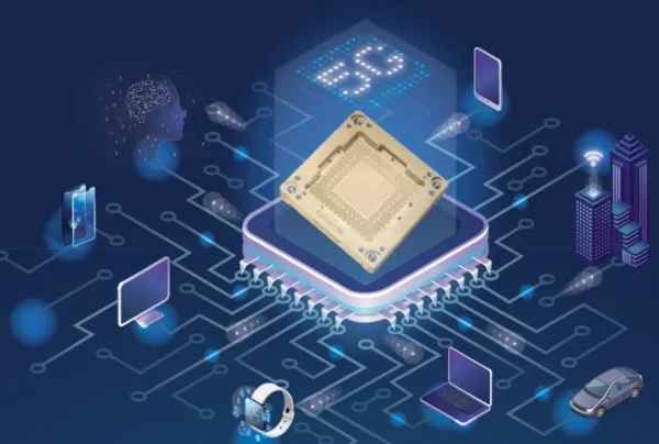
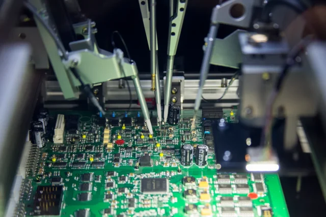
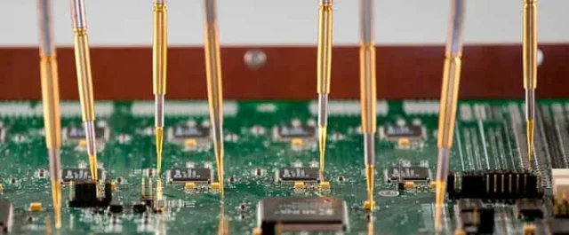
In the era of advanced semiconductor devices, accurate testing is critical for ensuring product quality and yield. Semiconductor Testing PCBs are specialized printed circuit boards designed to interface between integrated circuits (ICs) and automated test equipment (ATE), providing precise electrical connections, controlled impedance, and robust mechanical support.
These PCBs are fundamental to wafer-level testing, IC characterization, and functional verification, ensuring reliable, repeatable, and high-speed semiconductor testing.
What Is a Semiconductor Testing PCB?
A semiconductor testing PCB is a high-performance board that serves as the interface between the device under test (DUT) and the testing system. Its main functions include:
-
Routing high-density signals for high-pin-count ICs
-
Maintaining controlled impedance and low signal loss for high-speed or RF signals
-
Providing reliable mechanical support for probe cards, load boards, and test sockets
-
Ensuring repeatable and accurate measurement across multiple test cycles
By combining precision design and robust materials, semiconductor testing PCBs reduce measurement errors and improve test yield.
Key Features of Semiconductor Testing PCBs
-
Controlled Impedance and Signal Integrity – Essential for high-speed, RF, and mixed-signal ICs.
-
High-Density Routing – Supports modern ICs with thousands of pins and complex interconnections.
-
Multilayer Stackups – Enables separate power and ground planes to reduce noise and crosstalk.
-
Mechanical Reliability – Ensures accurate alignment with probe cards and test sockets.
-
Thermal Stability – Handles temperature variations during burn-in testing or extended high-power tests.
These features ensure semiconductor testing PCBs deliver accurate and reliable results under rigorous test conditions.
Materials and Stackup Considerations
Material choice directly impacts the performance and durability of semiconductor testing PCBs:
-
High-Tg FR-4 – Suitable for standard-speed test PCBs with moderate thermal stress.
-
Low-Loss Laminates – Critical for high-frequency or RF testing applications.
-
Hybrid Stackups – Combine cost-efficiency with electrical performance for advanced test requirements.
A well-planned stackup ensures consistent controlled impedance, minimal signal loss, and long-term reliability.
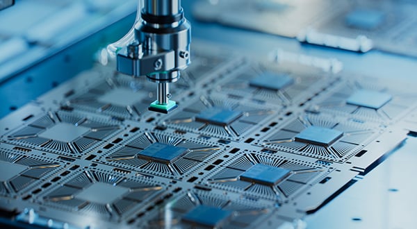
Applications of Semiconductor Testing PCBs
Semiconductor testing PCBs are used in:
-
Wafer-level functional and parametric testing
-
IC characterization and burn-in testing
-
Load boards, probe card interfaces, and test sockets in ATE systems
-
High-speed digital, mixed-signal, and RF testing
They are essential for reducing test errors, improving IC yield, and enabling faster time-to-market.
Choosing a Semiconductor Testing PCB Supplier
When selecting a semiconductor testing PCB manufacturer, consider:
-
Experience with high-pin-count, high-speed, and multilayer test PCB designs
-
Capability for controlled impedance, low-loss routing, and precise assembly
-
Support for prototype, small batch, and volume production
-
Quality control, electrical verification, and design consultation services
A reliable partner ensures consistent performance, repeatability, and high-quality test results.
Conclusion
Semiconductor Testing PCBs are a cornerstone of modern IC validation, providing high-density routing, controlled impedance, and reliable mechanical support. By ensuring accurate, repeatable, and high-speed testing, these PCBs improve semiconductor yield and product quality.
Partnering with an experienced semiconductor testing PCB manufacturer guarantees reliable performance, fast prototyping, and scalable production from early-stage validation to full-scale manufacturing.
