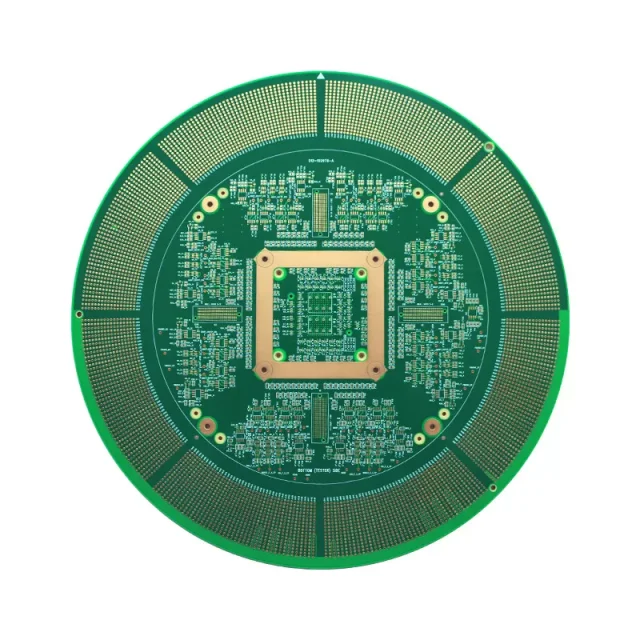
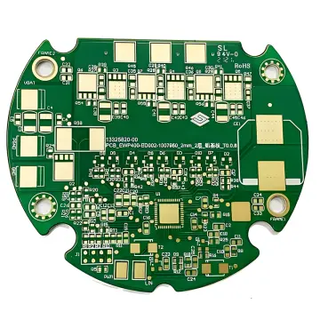
Semiconductor testing is a critical process that ensures device functionality, performance, and yield before products reach the market. Semiconductor testing PCBs serve as the electrical foundation of this process, enabling accurate signal transmission and stable power delivery across wafer test, IC test, and final test stages.
These specialized PCBs are designed to meet extreme electrical, mechanical, and reliability requirements.
Role of Semiconductor Testing PCBs in the Test Flow
A semiconductor testing PCB functions as the interface between the device under test and test equipment. Throughout the semiconductor test flow, these PCBs are used in:
-
Wafer-level probing and characterization
-
IC package testing and validation
-
Final functional and reliability testing
Each stage requires precise electrical performance and mechanical stability.
Electrical Requirements of Semiconductor Testing PCBs
To ensure accurate measurement, semiconductor testing PCBs must support:
-
Controlled impedance for high-speed and RF signals
-
Low crosstalk and minimal signal loss
-
Multiple power domains with low noise
-
Stable reference planes for repeatable results
These requirements directly affect test accuracy and yield.
High Pin Count and Dense Routing
Modern semiconductor devices often feature thousands of I/O connections. Semiconductor testing PCBs are engineered to:
-
Break out high pin count devices efficiently
-
Support fine-pitch connectors, sockets, and probe cards
-
Maintain signal integrity in dense multilayer layouts
High-density routing is essential for advanced semiconductor testing.
Material Selection and Stackup Design
Material choice plays a vital role in semiconductor testing PCB performance. Depending on test requirements, designs may use:
-
High-Tg FR-4 for general test applications
-
Low-loss laminates for high-speed or RF testing
-
Hybrid stackups to optimize cost and performance
Well-designed stackups ensure electrical stability across operating conditions.
Manufacturing and Quality Control
Producing reliable semiconductor testing PCBs requires advanced manufacturing processes, including:
-
Tight layer-to-layer registration
-
Controlled impedance fabrication
-
Electrical testing and signal verification
-
Strict quality inspection standards
Consistent manufacturing quality helps prevent false failures during testing.
Applications of Semiconductor Testing PCBs

Semiconductor testing PCBs are widely applied in:
-
Wafer test and probe card interfaces
-
ATE load boards and interface boards
-
High-speed IC characterization platforms
-
Final test and system-level validation
Each application demands precision, reliability, and repeatability.
Choosing a Semiconductor Testing PCB Partner
When selecting a semiconductor testing PCB manufacturer, consider:
-
Experience with ATE and semiconductor test hardware
-
Capability for multilayer and high pin count designs
-
Support for prototype, small batch, and volume production
-
Robust quality control and engineering support
A trusted partner ensures stable test performance across all stages.
Conclusion
Semiconductor testing PCBs are a cornerstone of reliable IC validation and production testing. By delivering controlled impedance, high pin count routing, and stable power integrity, these PCBs enable accurate, repeatable, and efficient semiconductor testing.
Partnering with an experienced semiconductor testing PCB supplier ensures quality, performance, and scalability from early development through mass production.
