As semiconductor devices advance toward higher speeds, higher pin counts, and smaller form factors, semiconductor testing PCBs have become a critical component in ensuring product quality and performance. These specialized PCBs form the electrical interface between integrated circuits and test equipment, enabling accurate signal transmission and reliable measurement during every test stage.
What Is a Semiconductor Testing PCB?
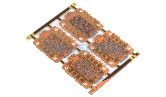
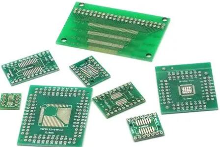
A semiconductor testing PCB is a purpose-built circuit board designed for IC testing processes such as wafer sort, final test, and characterization. Unlike standard PCBs, semiconductor testing PCBs must meet extremely tight electrical and mechanical tolerances to support precise test conditions.
They are commonly used in:
-
Automatic Test Equipment (ATE)
-
Load boards and interface boards
-
Probe cards and test sockets
Key Requirements of Semiconductor Testing PCBs
Semiconductor testing PCBs must handle a combination of demanding requirements, including:
-
High-speed digital and RF signal routing
-
Controlled impedance and low signal loss
-
High pin count device breakout
-
Multiple power and ground domains
Each requirement directly impacts test accuracy and repeatability.
Signal Integrity for Semiconductor Testing
Signal integrity is a top priority in semiconductor testing PCB design. These boards are engineered with:
-
Controlled impedance traces
-
Dedicated reference planes
-
Optimized stackup symmetry
Such features minimize crosstalk, reflection, and timing skew, ensuring reliable test results even at high data rates.
Power Integrity and Noise Control
Stable power delivery is essential during semiconductor testing. Semiconductor testing PCBs incorporate:
-
Low-impedance power planes
-
Short return paths
-
Effective decoupling strategies
This design approach reduces power noise and supports consistent device operation during testing.
PCB Materials and Stackup Design
Material selection plays a crucial role in semiconductor testing PCB performance. Typical designs may use:
-
High-Tg FR-4 for general testing
-
Low-loss laminates for high-speed or RF test boards
-
Hybrid stackups to balance performance and cost
Careful stackup planning ensures electrical stability across operating conditions.
Manufacturing Challenges of Semiconductor Testing PCBs
Producing high-quality semiconductor testing PCBs requires advanced fabrication capabilities, such as:
-
Fine-line and high-density routing
-
High aspect ratio vias
-
Tight layer registration control
-
Strict impedance and continuity testing
Consistent manufacturing quality is critical to avoid false test failures.
Applications of Semiconductor Testing PCBs
Semiconductor testing PCBs are widely used in:
-
IC functional and parametric testing
-
Wafer-level testing and probing
-
Final test and system-level validation
-
High-speed and mixed-signal semiconductor devices
Each application demands precision and reliability.
Selecting a Semiconductor Testing PCB Manufacturer
When choosing a semiconductor testing PCB supplier, consider:
-
Experience with ATE and IC test applications
-
Capability for controlled impedance PCB fabrication
-
Support for prototype and small batch builds
-
Strong quality control and testing processes
A reliable partner helps reduce test risk and shorten product validation cycles.
Conclusion
The semiconductor testing PCB is an essential element in modern IC development and production. With its focus on signal integrity, power stability, and manufacturing precision, it ensures accurate and repeatable semiconductor testing across all stages of validation.
Partnering with an experienced semiconductor testing PCB manufacturer enables higher test confidence, faster iteration, and improved overall yield.
