As semiconductor devices continue to scale in speed, complexity, and pin count, testing accuracy becomes critical. The Semiconductor Testing PCB serves as the core platform connecting devices under test (DUTs) with automated test equipment (ATE), enabling precise electrical characterization and reliable production testing.
High-quality semiconductor testing PCBs are essential for yield improvement and risk reduction.
What Is a Semiconductor Testing PCB?
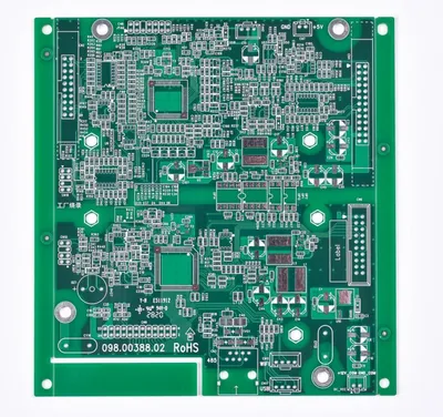
A Semiconductor Testing PCB is a specialized printed circuit board designed to support electrical testing of ICs and semiconductor devices throughout their lifecycle, including engineering validation, qualification, and volume production.
These PCBs must maintain stable electrical performance under high-speed, high-density, and repetitive test conditions.
Key Roles in the Semiconductor Test Flow
Semiconductor testing PCBs are used across multiple stages:
-
Engineering validation and characterization
-
Design verification testing (DVT)
-
Reliability and qualification testing
-
High-volume production testing
Each stage demands consistent signal and power integrity.
Signal Integrity for High-Speed Semiconductor Testing
Modern semiconductor devices operate at extremely high data rates. Semiconductor testing PCBs focus on:
-
Controlled impedance routing
-
Low-loss dielectric materials
-
Minimization of crosstalk and reflection
Accurate signal behavior ensures valid test results.
Power Integrity and Noise Control
Stable power delivery is critical in semiconductor testing. Key design considerations include:
-
Dedicated power and ground planes
-
Optimized decoupling capacitor placement
-
Low-inductance current paths
These measures prevent noise-induced test errors.
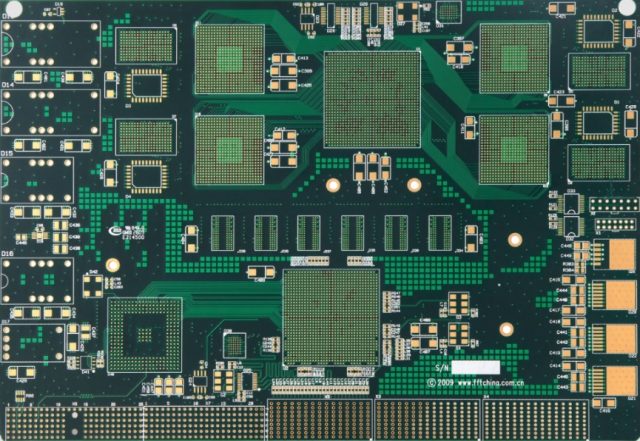
High Density and High Pin Count Support
Semiconductor testing PCBs often handle:
-
Thousands of signal connections
-
Fine-pitch interfaces and sockets
-
Complex multilayer routing
High layer count and HDI structures are commonly required.
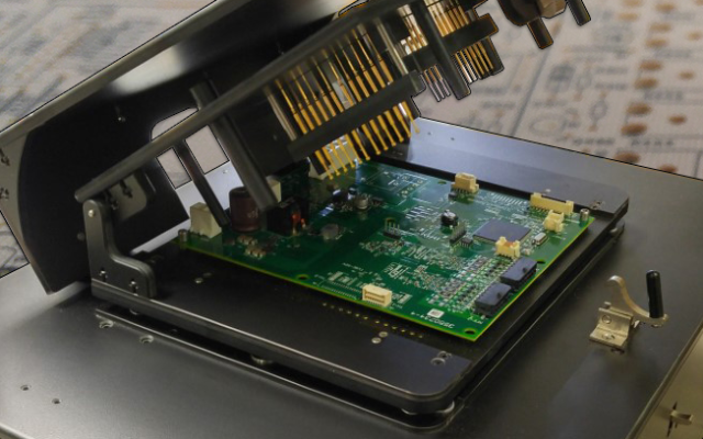
Mechanical and Thermal Reliability
Testing environments expose PCBs to:
-
Frequent socket insertions
-
Thermal cycling
-
Long test durations
Robust materials and construction ensure long-term reliability.
Manufacturing and Quality Requirements
Producing semiconductor testing PCBs requires:
-
Tight fabrication tolerances
-
Advanced multilayer and HDI processes
-
Comprehensive electrical and impedance testing
Strict quality control ensures repeatable performance.
Typical Types of Semiconductor Testing PCBs
The semiconductor testing ecosystem includes:
-
ATE Test PCBs
-
Load Board PCBs
-
Probe Card PCBs
-
Test Socket PCBs
Each type supports specific test functions.
Choosing a Semiconductor Testing PCB Manufacturer
When selecting a semiconductor testing PCB supplier, consider:
-
Experience with test and semiconductor applications
-
Capability for high layer count and controlled impedance
-
Engineering support for DFM and SI/PI optimization
-
Ability to support prototype, small batch, and production
An experienced partner improves test stability and yield.
Conclusion
The Semiconductor Testing PCB is a critical enabler of accurate, repeatable, and scalable semiconductor testing. By ensuring signal integrity, power stability, and mechanical reliability, these PCBs support confident device validation and high-volume production testing.
Partnering with a specialized semiconductor testing PCB manufacturer helps ensure consistent performance across the entire test lifecycle.
