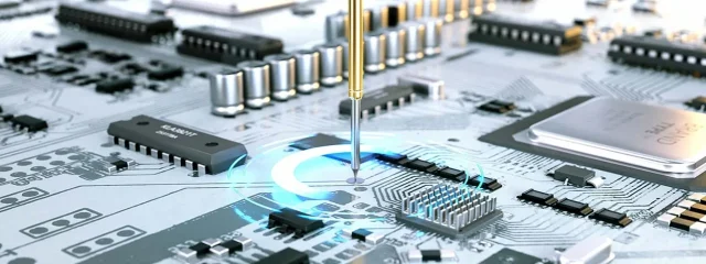
In semiconductor manufacturing, testing is a critical step that directly affects product quality and yield. The Semiconductor Test PCB serves as the electrical interface between the device under test and automated test systems, enabling accurate, repeatable, and high-speed measurements throughout the testing lifecycle.
A professionally engineered semiconductor test PCB ensures test results truly reflect device performance.
What Is a Semiconductor Test PCB?
A semiconductor test PCB is a specialized printed circuit board designed for electrical testing of semiconductor devices at various stages, including:
-
Wafer-level testing
-
Package-level functional testing
-
Reliability and stress testing
These boards are optimized for precision rather than cost.
Why Semiconductor Test PCBs Are Critical
Modern semiconductor devices feature:
-
High pin counts
-
High-speed interfaces
-
Tight electrical margins
Semiconductor test PCBs provide the controlled environment required to measure performance accurately.
Signal Integrity Requirements in Semiconductor Test PCBs
Signal integrity is fundamental in semiconductor testing. Key design goals include:
-
Controlled impedance routing
-
Minimal signal skew
-
Reduced crosstalk and noise
Dedicated reference planes help maintain measurement accuracy.
Power Integrity and Grounding Strategy
Stable power delivery is essential during functional and parametric testing. Semiconductor test PCBs typically use:
-
Solid power and ground planes
-
Low-inductance decoupling networks
-
Optimized current return paths
These strategies prevent false failures during testing.
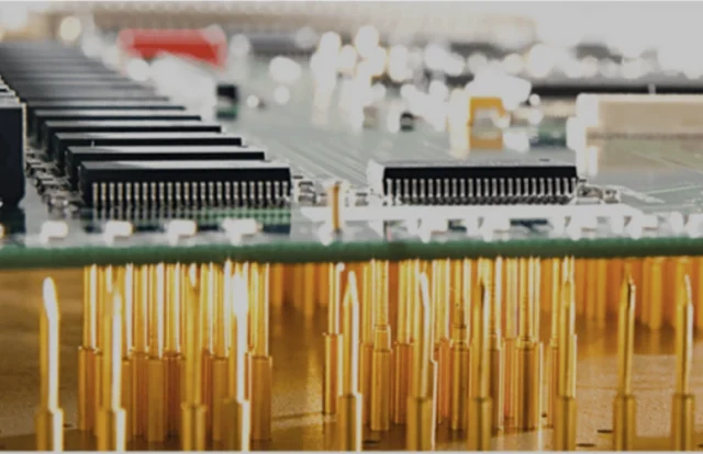
High-Density Interconnect and Via Design
To accommodate high pin counts, semiconductor test PCBs often incorporate:
-
Fine-line routing
-
Blind and buried vias
-
Via reinforcement for repeated use
Advanced interconnects improve routing efficiency and reliability.
Material Selection and Stackup Design
Material choice depends on test frequency and environment. Common options include:
-
High-Tg FR-4 for structural stability
-
Low-loss laminates for high-speed signals
-
Hybrid stackups for balanced performance and cost
Proper stackup design ensures consistent impedance and mechanical stability.
Manufacturing Precision and Quality Control
Fabrication of semiconductor test PCBs requires:
-
Tight dimensional tolerances
-
Accurate layer registration
-
Electrical and impedance testing
Strict quality control ensures repeatable test results across multiple boards.
Typical Applications of Semiconductor Test PCBs
Semiconductor test PCBs are widely used in:
-
Automated test equipment (ATE) systems
-
Probe cards and load boards
-
Device characterization platforms
-
Reliability and burn-in testing
Each application demands high accuracy and durability.
Choosing a Semiconductor Test PCB Manufacturer
When selecting a semiconductor test PCB supplier, consider:
-
Experience with test-specific PCB designs
-
Capability for high-density and high-speed boards
-
Strong process control and traceability
-
Engineering collaboration during DFM review
The right partner reduces development risk and test downtime.
Conclusion
A Semiconductor Test PCB is a critical enabler of accurate device validation and production testing. Through precise design, controlled manufacturing, and rigorous quality assurance, these PCBs ensure reliable and repeatable semiconductor test results.
Working with an experienced semiconductor test PCB manufacturer is essential for maintaining test integrity across the entire product lifecycle.
