What Is a Semiconductor Test PCB?
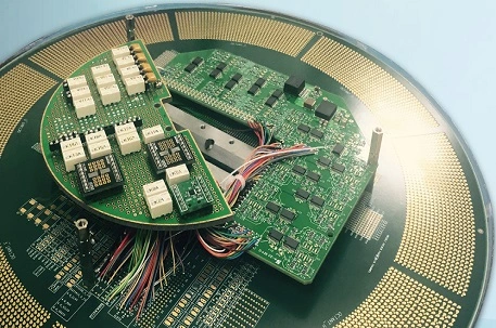
A Semiconductor Test PCB is a printed circuit board specifically designed to test, validate, and measure semiconductor devices under controlled conditions. These PCBs are used in automated test equipment (ATE), burn-in systems, and R&D labs to verify the performance and reliability of ICs before mass production.
Unlike standard PCBs, Semiconductor Test PCBs are engineered to handle high pin-counts, precise signal routing, and high-speed or high-frequency signals, ensuring accurate measurement results.
Key Design Considerations for Semiconductor Test PCB
Designing a Semiconductor Test PCB requires attention to the following factors:
-
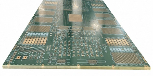
High pin-count routing
Supports complex IC packages such as BGA, QFP, and CSP. -
Controlled impedance traces
Ensures signal integrity for high-speed semiconductors. -
Durable test points
Withstands repeated probing and connection to test equipment. -
Thermal management
Proper copper planes and vias dissipate heat during high-current or burn-in testing. -
Minimal crosstalk and noise
Critical for accurate measurement of analog, digital, and mixed-signal ICs.
Materials and Manufacturing Considerations
Semiconductor Test PCBs often use specialized materials for precision and reliability:
-
High-performance FR-4 laminates
For standard IC testing. -
PTFE or Rogers laminates
For high-frequency or RF semiconductor testing. -
Metal-core or ceramic substrates
For high-current or high-temperature applications.
Manufacturing considerations include:
-
Accurate microvia and via-in-pad technology
Supports high-density IC packages. -
Precise layer registration and lamination
Prevents warpage and ensures dimensional stability. -
Surface finishes
ENIG, hard gold, or immersion silver for reliable probing. -
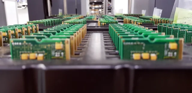
Electrical and functional testing
Confirms PCB performance before use in test systems.
Advantages of Semiconductor Test PCB
Using a Semiconductor Test PCB provides multiple benefits:
-
High-accuracy IC testing
-
Repeatable and reliable measurement results
-
Support for high-speed, high-frequency devices
-
Early detection of failures in semiconductor devices
-
Improved yield and product quality
These advantages make Semiconductor Test PCBs essential for semiconductor manufacturing and R&D.
Applications of Semiconductor Test PCB
Semiconductor Test PCBs are widely used in:
-
IC and microcontroller functional testing
-
Automated Test Equipment (ATE)
-
Burn-in testing for reliability verification
-
High-frequency RF semiconductor validation
-
Power semiconductor module testing
They are indispensable in semiconductor R&D, QA, and production testing.
Conclusion
A Semiconductor Test PCB is a critical tool for ensuring high-precision testing, reliable measurements, and product quality in semiconductor development and production. With careful design, high-quality materials, and precision manufacturing, Semiconductor Test PCBs provide accurate results, reduce production risks, and improve overall device reliability.
Partnering with an experienced Semiconductor Test PCB manufacturer ensures robust, high-quality boards capable of supporting advanced IC testing and R&D workflows.
