
Semiconductors are the foundation of modern electronic systems, powering everything from smartphones and industrial automation equipment to automotive electronics, medical devices, AI servers, and communication infrastructure. Behind every integrated circuit (IC) is a highly sophisticated manufacturing process that combines advanced materials science, precision engineering, and nanometer-scale fabrication technologies.
The semiconductor manufacturing process involves hundreds of tightly controlled steps, transforming a pure silicon wafer into a functional integrated circuit. Once fabricated, semiconductor devices are packaged, tested, and assembled onto printed circuit boards (PCBs) to form complete electronic products.
For companies involved in PCB manufacturing and PCBA assembly, understanding the semiconductor production flow helps optimize PCB design, package selection, thermal management, and manufacturing compatibility.
This article provides an overview of the semiconductor manufacturing process, including key production stages, major technologies, process flow, and its relationship with PCB and PCBA manufacturing.
1. What Is Semiconductor Manufacturing?

Semiconductor manufacturing is the process of fabricating integrated circuits on silicon wafers using a sequence of physical and chemical processes.
The objective is to build millions—or even billions—of microscopic transistors, resistors, capacitors, and interconnections that perform specific electronic functions.
Modern semiconductor fabrication requires:
- Ultra-clean cleanrooms
- Nanometer-scale lithography
- High-precision deposition and etching
- Automated inspection and testing
Today’s advanced ICs may contain tens of billions of transistors fabricated on process nodes below 5 nm.
2. Semiconductor Manufacturing Flow Chart
A simplified manufacturing flow is shown below:
Silicon Raw Material
↓
Silicon Crystal Growth
↓
Wafer Slicing & Polishing
↓
Wafer Fabrication
(Photolithography, Deposition,
Etching, Ion Implantation)
↓
Wafer Inspection
↓
Wafer Testing
↓
Wafer Dicing
↓
IC Packaging
↓
Final Testing
↓
PCB Assembly (PCBA)
↓
Electronic Product
3. Major Steps in Semiconductor Manufacturing
Step 1: Silicon Purification
The process begins with quartz sand, which contains silicon dioxide (SiO₂).
Through multiple purification processes, silicon is refined into:
- Electronic-grade silicon
- Purity exceeding 99.9999999% (9N or higher)
This extremely pure material is essential for semiconductor fabrication.
Step 2: Single Crystal Growth
Purified silicon is melted and formed into a single crystal ingot.
The most common method is the:
- Czochralski (CZ) Process
The resulting silicon crystal provides:
- Uniform crystal orientation
- High electrical consistency
- Excellent material quality
Step 3: Wafer Manufacturing
The crystal ingot is:
- Sliced into thin wafers
- Ground
- Polished
- Cleaned
Typical wafer diameters include:
- 200 mm (8-inch)
- 300 mm (12-inch)
Each wafer serves as the substrate for hundreds or thousands of ICs.
4. Wafer Fabrication Process
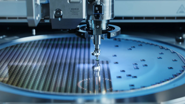
Wafer fabrication is the most complex stage of semiconductor manufacturing.
A modern fabrication process may involve 500–1,500 individual process steps.
4.1 Oxidation
A thin silicon dioxide layer is grown on the wafer surface.
Functions include:
- Electrical insulation
- Gate dielectric formation
- Surface protection
4.2 Photolithography
Photolithography transfers circuit patterns onto the wafer.
The process includes:
- Apply photoresist.
- Align the photomask.
- Expose to ultraviolet (UV) light.
- Develop the pattern.
Modern technologies include:
- Deep Ultraviolet (DUV)
- Extreme Ultraviolet (EUV)
Photolithography largely determines:
- Feature size
- Circuit density
- Manufacturing precision
4.3 Etching
After lithography, unwanted material is removed.
Common methods include:
- Wet etching
- Dry plasma etching
Etching creates:
- Circuit patterns
- Trenches
- Contact openings
4.4 Thin Film Deposition
Thin layers of conductive or insulating materials are deposited.
Common techniques include:
- Chemical Vapor Deposition (CVD)
- Physical Vapor Deposition (PVD)
- Atomic Layer Deposition (ALD)
Materials include:
- Silicon nitride
- Silicon dioxide
- Copper
- Tungsten
4.5 Ion Implantation
Impurity atoms are implanted into silicon.
Purpose:
- Form N-type regions
- Form P-type regions
These doped regions create:
- Transistors
- Diodes
- CMOS structures
4.6 Chemical Mechanical Planarization (CMP)
CMP smooths the wafer surface after multiple fabrication layers.
Benefits include:
- Flat surfaces
- Improved lithography accuracy
- Better multilayer alignment
4.7 Metallization
Metal interconnects connect millions of transistors together.
Modern ICs typically use:
- Copper interconnects
- Multiple metal layers
- Low-k dielectric materials
Advanced chips may contain 10–20 or more metal layers.
5. Wafer Inspection and Testing
Throughout fabrication, wafers undergo extensive inspection.
Common inspection methods include:
- Optical inspection
- Scanning electron microscopy (SEM)
- Defect inspection
- Overlay measurement
Electrical testing verifies:
- Device functionality
- Parametric performance
- Yield
Early defect detection helps reduce manufacturing costs.
6. Wafer Dicing
Once fabrication is complete:
- Individual dies are separated from the wafer using precision saws or laser cutting.
Each die becomes an individual semiconductor device.
7. IC Packaging
Packaging protects the silicon die while providing electrical connections to the outside world.
Common package types include:
Wire Bond Package
Advantages:
- Mature technology
- Lower cost
Applications:
- Consumer electronics
- Industrial electronics
Flip-Chip Package
Advantages:
- Higher electrical performance
- Better thermal performance
- Shorter signal paths
Applications:
- CPUs
- GPUs
- AI processors
Ball Grid Array (BGA)
Advantages:
- High pin count
- Excellent electrical performance
- Compact footprint
Applications:
- Communication devices
- Automotive electronics
- High-speed processors
Chip Scale Package (CSP)
Advantages:
- Miniaturization
- Lightweight design
Applications:
- Mobile devices
- Wearables
8. Final Testing
Packaged ICs undergo comprehensive testing, including:
- Functional testing
- Speed testing
- Power consumption testing
- Thermal testing
- Reliability testing
Only qualified devices proceed to shipment.
9. Relationship Between Semiconductor Manufacturing and PCB Assembly
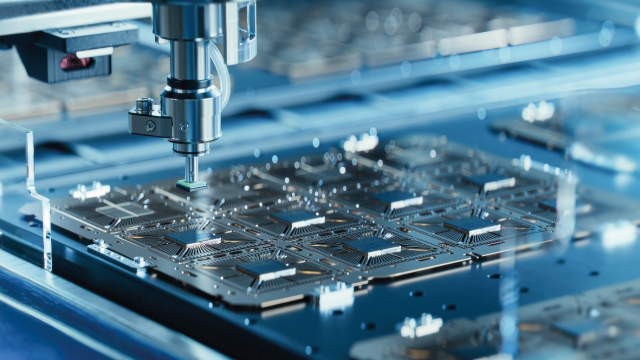
Although semiconductor fabrication and PCB manufacturing are different processes, they are closely connected.
Once packaged, semiconductor devices are assembled onto PCBs through SMT or THT processes.
PCB design directly affects semiconductor performance through:
Signal Integrity
High-speed ICs require:
- Controlled impedance routing
- Differential pair matching
- Low-noise layouts
Power Integrity
Proper PCB design ensures:
- Stable power delivery
- Reduced voltage ripple
- Effective decoupling
Thermal Management
High-performance processors generate significant heat.
PCB solutions may include:
- Thermal vias
- Heavy copper layers
- Metal-core PCBs
- Heat sinks
Manufacturability (DFM)
PCB layout should consider:
- Package type
- Pad geometry
- Solder joint reliability
- Assembly tolerances
Early DFM review helps improve production yield and long-term reliability.
10. Emerging Semiconductor Technologies
The semiconductor industry continues to evolve with innovations such as:
- 3D IC packaging
- Chiplet architectures
- Advanced heterogeneous integration
- Fan-Out Wafer-Level Packaging (FOWLP)
- 2.5D packaging
- Silicon photonics
- Gallium Nitride (GaN) power devices
- Silicon Carbide (SiC) power semiconductors
These technologies place increasing demands on PCB design, requiring improved:
- Signal integrity
- Thermal performance
- High-density interconnection (HDI)
- Advanced PCB materials
Conclusion
Semiconductor manufacturing is one of the world’s most advanced production processes, combining hundreds of precision fabrication steps to create highly integrated electronic devices.
From silicon purification and wafer fabrication to packaging and final testing, every stage directly influences chip performance, reliability, and manufacturing yield.
For PCB and PCBA manufacturers, understanding semiconductor manufacturing helps optimize board design, package compatibility, thermal management, and production readiness. As semiconductor technologies continue advancing toward higher integration and faster operating speeds, close collaboration between semiconductor packaging and PCB engineering will become increasingly important for delivering reliable, high-performance electronic systems.
