Engineering Reliable RF Performance with KKPCB’s Hybrid Lamination Expertise
As 5G and radar systems advance toward higher frequencies (24–77 GHz) and more compact multilayer designs, engineers increasingly choose Rogers RO4350B PCB for its stable dielectric properties, low loss, and compatibility with standard FR-4 processes.
Yet, when moving to hybrid stackups—mixing RO4350B with FR-4, prepregs, or ceramic layers—the lamination process becomes the key determinant of yield, impedance uniformity, and long-term reliability.
This article explores how KKPCB’s controlled hybrid lamination process enables repeatable, scalable production for complex RF boards transitioning from prototype to automotive-grade mass manufacturing.
1. Why Hybrid Stackups Have Become the Standard for RO4350B Designs
In real-world RF modules, performance and cost must coexist.
A full-Rogers stackup delivers excellent dielectric precision but is expensive and mechanically less versatile.
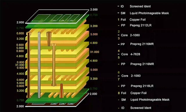
That’s why most 5G antenna, automotive radar, and satellite transceiver boards use hybrid stackups—where RO4350B handles RF paths, and FR-4 or low-Dk prepregs manage power, control, and mechanical stability.
| Layer | Material | Function |
|---|---|---|
| Top | RO4350B (0.254 mm) | RF microstrip / antenna layer |
| Core | FR-4 / Low-Dk Prepreg | Power & control routing |
| Bottom | RO4350B (0.508 mm) | RF feed / phase line |
This configuration optimizes cost and RF performance, but introduces CTE mismatch, resin flow inconsistency, and impedance drift—factors that can reduce yield if not tightly controlled.
2. Key Lamination Challenges in RO4350B Hybrid Structures
(1) CTE Mismatch Between RO4350B and FR-4
RO4350B (≈ 11 ppm/°C X/Y) and FR-4 (≈ 17 ppm/°C) expand at different rates.
This thermal mismatch can cause warpage, resin squeeze-out, or interlayer cracking during heating and cooling cycles.
KKPCB Solution:
-
Vacuum-assisted lamination with < 2 °C/min controlled heating rate
-
Balanced press lay-ups to equalize thermal expansion
-
Real-time temperature monitoring to maintain dielectric planarity
(2) Resin Flow and Prepreg Compatibility
Different resin rheology between RO4350B and standard FR-4 prepregs can cause voids, dry spots, or poor adhesion—directly increasing RF loss.
KKPCB Solution:
-
Use of Rogers-approved low-flow prepregs or custom bonding films
-
Resin-flow simulation to predict squeeze zones
-
Micro-etch or plasma activation on RO4350B surfaces for improved bonding
(3) Impedance Drift During Lamination
Small variations in resin thickness or lamination pressure shift dielectric spacing—altering the characteristic impedance of RF traces.
-
In-line VNA impedance verification on every production batch
-
± 5 µm etching precision for consistent conductor geometry
-
Tight CTE control (< ± 3 °C variance) across press cycles
(4) Multi-Material Lamination Voids
Interfaces between dissimilar materials can trap air, causing localized reflections or hot spots at mmWave frequencies.
-
Multi-stage vacuum lamination with pre-bake moisture removal
-
Controlled pressure ramping to avoid air entrapment
-
Optical / ultrasonic inspection after lamination for void detection
3. Case Study: 24 GHz Automotive Radar Hybrid Stackup
A Tier-1 automotive supplier partnered with KKPCB to mass-produce a 6-layer radar transceiver PCB combining RO4350B (RF layers) with FR-4 structural cores.
Design Challenges
-
Maintain ± 5 % impedance tolerance across hybrid transitions
-
Prevent delamination under −40 °C to +125 °C cycling
-
Control warpage < 0.15 mm per panel
KKPCB Engineering Approach
-
Custom RO4350B + FR-4 + low-flow prepreg stackup
-
Stepwise lamination profile: 180 °C / 45 min / 200 psi
-
Thermal-stress simulation (IPC-TM-650) validation
| Parameter | Before Optimization | After KKPCB Process |
|---|---|---|
| Impedance Variation | ± 12 % | ± 3 % |
| Delamination Rate | 7 % | < 0.5 % |
| Module Yield | 86 % | 97 % |
Engineering Insight:
During initial builds, microscopic resin voids near via pads caused > 10 % impedance drift.
By refining the lamination ramp rate and introducing moisture pre-bake, KKPCB eliminated the issue completely in production.
4. Best Practices for Reliable Hybrid RO4350B Stackups
-
Maintain dielectric balance; avoid symmetrical FR-4 pairing above/below RF layers
-
Use Rogers 4450F prepreg when Dk matching is critical
-
Limit total lamination cycles (< 2) to avoid dielectric drift
-
Perform CTE simulation in early stackup design
-
Validate impedance and dielectric thickness under real production conditions
5. KKPCB’s Advanced Lamination Process Control
KKPCB’s hybrid PCB production line is designed for repeatability, yield, and mmWave stability, featuring:
-
± 3 °C temperature uniformity across lamination plates
-
Controlled cooling gradient to reduce interlayer stress
-
Automated resin-flow & void detection
-
IPC Class 3 / IATF 16949-certified automotive-grade RF production
-
In-house RF impedance lab with VNA calibration up to 110 GHz
Conclusion – From Prototype Stability to Scalable RF Reliability
Scaling from prototype to mass production exposes hidden hybrid lamination risks—resin mismatch, CTE deviation, impedance drift, and void formation.
With KKPCB’s hybrid lamination expertise, these variables are characterized, modeled, and controlled, ensuring repeatable RF performance, low defect rates, and automotive-grade durability.
Developing RF or 5G hybrid boards?
KKPCB’s engineering team can help you:
-
Simulate and validate optimal stackup configurations
-
Optimize lamination profiles and Dk verification
-
Conduct RF impedance and reliability testing for production
Contact KKPCB Engineering Support to review your hybrid lamination design or request a DFM evaluation.
