Redefining PCB Reliability in High-Power 5G Amplifiers
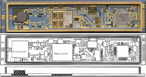
As 5G base station architectures evolve toward massive MIMO and mmWave deployment (24–39 GHz), power amplifier (PA) modules have become one of the most thermally and electrically demanding components in the RF chain.
Each PA channel can handle continuous power levels above 10 W, generating localized heat flux exceeding 10–15 W/cm². PCB materials must therefore combine low loss, dimensional stability, and superior thermal management—all without compromising manufacturability or cost efficiency.
Rogers RO4003C has become the benchmark material for these applications.
With its low loss tangent (Df = 0.0027 @ 10 GHz), stable dielectric constant (Dk = 3.55 ± 0.05), and high Tg (> 280°C), it provides a reliable dielectric foundation for high-power, multi-layer RF amplifier designs.
However, thermal reliability in PA systems is not determined by Dk alone—it depends on the entire stackup architecture, heat path continuity, and resin-to-metal interface control during production.
That’s where KKPCB’s thermal engineering workflow ensures consistent high-frequency performance from prototype validation to mass manufacturing.
Key Thermal Challenges in RO4003C Power Amplifier PCBs
| Challenge | Engineering Impact | Design Concern |
|---|---|---|
| Localized Hotspots Under Transistor Pads | Heat accumulation → gain compression, frequency drift | Uneven copper distribution, resin voids |
| Dielectric Loss at High RF Power | Excessive heat from tanδ losses | Increased board temperature and long-term Dk drift |
| CTE Mismatch Between Copper and Dielectric | Mechanical stress during power cycling | Microcrack or delamination under solder pads |
| Incomplete Thermal Path to Baseplate | Poor heat spreading efficiency | Reduced PA output power, shorter MTBF |
KKPCB addresses these issues through integrated stackup simulation, embedded thermal vias, and hybrid laminate optimization, achieving both thermal conductivity and RF linearity.
KKPCB Thermal Management Framework
1. Stackup Design for Heat Spreading and Dk Stability
Typical 5G PA modules use 4–6 layer hybrid designs, integrating RO4003C for RF transmission and low-Dk prepregs or metal-backed substrates for heat spreading.
Optimized Stackup Example:
| Layer | Material | Function |
|---|---|---|
| Top | RO4003C 0.203 mm | RF power trace and transistor interface |
| Core | RO4003C + Cu plane | Signal routing and heat conduction |
| Base | Aluminum or Cu baseplate | Mechanical support and thermal sink |
-
Layer symmetry for CTE balance
-
Controlled Cu roughness (Ra < 1.5 µm) for thermal contact
-
Via filling with high-Tg resin for uniform heat conduction
2. Embedded Thermal Via Networks
KKPCB engineers apply via density optimization beneath transistor and matching networks to minimize junction temperature rise.
For a 5G 28 GHz PA test vehicle, results showed:
| Parameter | Standard Layout | KKPCB Optimized Layout |
|---|---|---|
| Max Junction Temp (Tj) | 148°C | 121°C |
| Gain Degradation | –0.6 dB | –0.1 dB |
| MTBF | 10,000 hr | > 35,000 hr |
Process Note:
Via drill precision (±25 µm) and resin backfill uniformity (<2 %) were critical to maintaining thermal conduction and impedance consistency at mmWave frequencies.
3. Lamination and Copper Adhesion Reliability
In hybrid stackups where RO4003C interfaces with FR-4 or aluminum base, CTE mismatch becomes a major reliability concern.
KKPCB employs:
-
Stepwise lamination profiles (180°C / 60 min / 200 psi)
-
Surface micro-etch & plasma activation to improve adhesion
-
Thermal cycling test (–40°C ↔ +150°C, 1,000 cycles) with no delamination or crack propagation
Result:
Post-test impedance drift within ±3%, confirming mechanical and electrical integrity.
4. Thermal and RF Reliability Validation
KKPCB’s in-house RF & thermal lab validates every production lot under combined power and temperature stress conditions:
| Test Type | Condition | Evaluation Metric |
|---|---|---|
| RF Power Cycling | 20 W, 10⁵ cycles | Gain compression < 0.2 dB |
| Thermal Shock | –55°C to +125°C, 500 cycles | No delamination / phase shift < 1° |
| High-Temp Aging | 150°C × 1,000 hr | Df drift < 0.0002 |
| 85/85 Humidity | 85°C / 85% RH × 1,000 hr | Moisture absorption < 0.1% |
These tests ensure that RO4003C-based PA boards meet telecom-grade reliability (IEC 60068 / AEC-Q200) standards.
6. Case Study: 28 GHz 5G Macro Base Station PA Board
A global telecom OEM collaborated with KKPCB to optimize its 28 GHz high-power amplifier module.
The design combined RO4003C with Cu base for efficient heat spreading.
Project Goals:
-
Maintain thermal resistance < 1.2°C/W
-
Impedance variation ≤ ±5%
-
Output stability over 10,000 hours operation
KKPCB Results:
-
Peak Tj reduction: –27°C
-
Df stability: 0.0027 → 0.0028 after 1,000 hr @150°C
-
RF yield improvement: +9.2% across 12 lots
Engineering Takeaways
To ensure stable performance in high-power RF systems, KKPCB recommends:
-
Integrate thermal vias directly beneath power transistors with 1.0 mm pitch.
-
Use RO4003C + Cu base hybrids to balance RF stability and thermal efficiency.
-
Maintain symmetric stackup to minimize CTE-induced warpage.
-
Conduct combined RF–thermal stress tests during qualification.
-
Verify Df and Dk drift post-aging before volume production.
KKPCB’s Manufacturing & Reliability Capabilities
-
IPC Class 3 / IATF 16949 certified
-
±3°C lamination temperature control
-
Real-time impedance verification (VNA up to 110 GHz)
-
Automated X-ray and C-SAM inspection
-
Accelerated life testing (thermal, humidity, vibration)
KKPCB’s high-frequency PCB production integrates RF electrical validation, thermal path modeling, and materials compatibility control, ensuring consistent reliability for telecom and aerospace customers.
Conclusion — Proven Thermal and RF Reliability with RO4003C
RO4003C PCBs combine low loss, stable dielectric properties, and strong thermal durability, making them ideal for 5G base station PA modules and other high-power RF systems.
Through KKPCB’s hybrid lamination expertise and thermal reliability testing, OEMs can achieve long-term RF stability, reduced failure rates, and scalable production quality.
Partner with KKPCB for RO4003C High-Power PCB Solutions
KKPCB Engineering Team offers:
-
Custom PA thermal design & simulation
-
RF impedance verification up to 110 GHz
-
Long-term reliability testing and AEC-Q qualification support
Contact KKPCB Engineering Support to discuss your 5G PA or RF power module project.
