What Is an RF Test PCB?
An RF Test PCB is a specialized printed circuit board used to test, validate, and characterize RF and microwave circuits under controlled and repeatable conditions. RF Test PCBs are widely used to measure key RF parameters such as insertion loss, return loss, impedance matching, phase stability, and signal integrity.
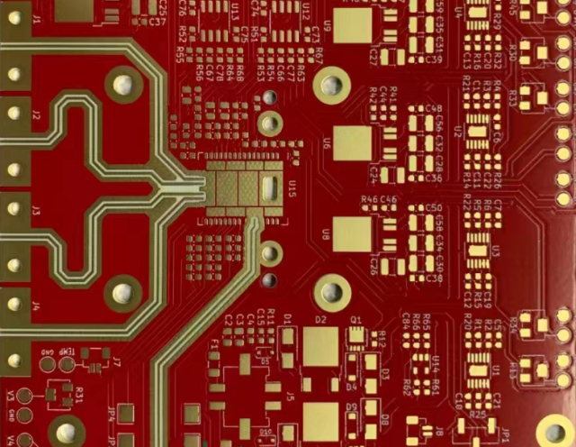
Compared with standard PCBs, an RF Test PCB requires strict impedance control, low-loss materials, precision layout, and stable grounding, ensuring test results are accurate and consistent.
Key Design Requirements for RF Test PCB
High-quality RF Test PCB design is critical for reliable RF measurement. Key requirements include:
-
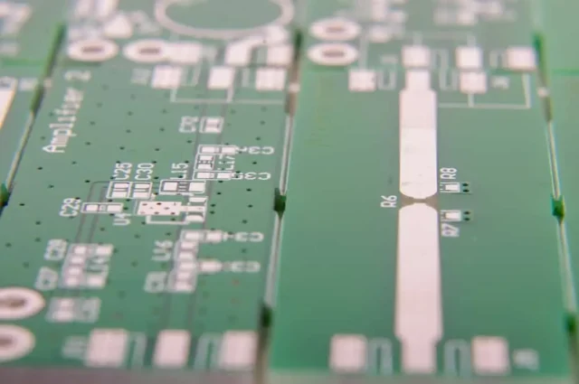
Controlled impedance routing
Typically 50Ω or 75Ω transmission lines with tight tolerance. -
Optimized RF trace layout
Short, straight traces minimize reflection and attenuation. -
Via transition optimization
Reduced via stubs and proper ground via stitching improve RF continuity. -
Connector launch accuracy
Precise SMA, SMP, 2.92 mm, or other RF connector interfaces. -
Grounding and shielding design
Solid reference planes reduce EMI and external interference.
These factors directly affect RF Test PCB performance and measurement accuracy.
Materials for RF Test PCB
Material selection plays a critical role in RF Test PCB performance. Common materials include:
-
Rogers PCB materials (RO4350B, RO4003C, RT/duroid series)
Low dielectric loss and stable Dk for RF testing. -
Taconic PCB materials
Excellent for microwave and high-frequency RF Test PCBs. -
PTFE-based laminates
Ideal for high-frequency and millimeter-wave testing. -
High-performance FR-4 (limited use)
Suitable for lower-frequency RF Test PCB applications.
Low Df and stable dielectric properties ensure repeatable RF test results.
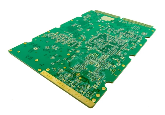
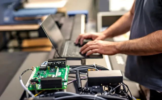
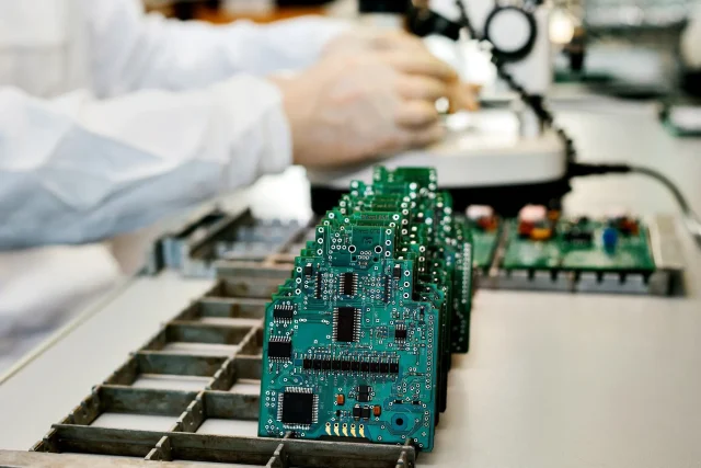
RF Test PCB Manufacturing Considerations
Manufacturing an RF Test PCB requires higher precision than standard PCB production:
-
Tight impedance tolerance control (±5% or better)
-
High-precision etching for RF trace accuracy
-
Smooth copper surface treatment to reduce conductor loss
-
Accurate layer alignment in multilayer RF Test PCBs
-
Impedance, electrical, and RF performance testing
Experienced RF Test PCB manufacturers ensure consistency across prototype and volume builds.
Advantages of Using RF Test PCB
Using a dedicated RF Test PCB provides clear advantages:
-
High measurement accuracy and repeatability
-
Reduced RF signal loss and reflection
-
Improved signal integrity in RF testing
-
Reliable evaluation of RF components and modules
-
Greater confidence before mass production
A well-designed RF Test PCB minimizes external variables during RF and microwave testing.
Applications of RF Test PCB
RF Test PCBs are widely used in:
-
RF module and antenna testing
-
5G, Wi-Fi, and wireless communication systems
-
Microwave and millimeter-wave circuit validation
-
Automotive radar and ADAS testing
-
Aerospace and defense RF electronics
-
Automated test equipment (ATE)
As operating frequencies continue to increase, RF Test PCBs become increasingly critical.
RF Test PCB vs Standard PCB
Compared to standard PCBs, RF Test PCBs feature:
-
Much tighter impedance control
-
Lower dielectric loss materials
-
Optimized RF routing and grounding
-
Higher manufacturing precision
These differences make RF Test PCB essential for accurate RF measurement and validation.
Conclusion
An RF Test PCB is a key component for achieving accurate, repeatable, and reliable RF and microwave testing. From material selection and impedance control to precision manufacturing, every detail directly impacts test performance.
Choosing an experienced RF Test PCB supplier ensures stable RF performance, reduced measurement uncertainty, and dependable validation for advanced RF applications.
