What Is an RF Test PCB?
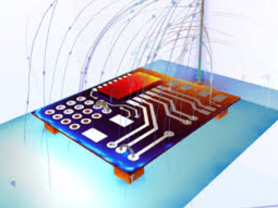
An RF Test PCB is a printed circuit board specifically designed for radio-frequency signal testing, measurement, and validation. RF Test PCBs are widely used in RF module verification, wireless communication testing, semiconductor characterization, and production testing.
Compared with standard application PCBs, RF Test PCBs focus on measurement accuracy, signal integrity, repeatability, and low signal loss, ensuring reliable RF test results.
Key Requirements for RF Test PCB
A high-quality RF Test PCB must meet strict technical requirements:
-
Low dielectric and conductor loss
Ensures accurate RF signal measurement. -
Precise impedance control (typically 50Ω / 75Ω)
Critical for RF trace and connector matching. -
Stable dielectric constant (Dk)
Maintains consistency across frequency ranges. -
Excellent RF connector integration
Supports SMA, SMP, K-type, and other RF connectors. -
Repeatability and reliability
Ensures consistent test results over multiple cycles.
These requirements are essential for RF testing accuracy.
Material Selection for RF Test PCB
Material choice directly impacts RF Test PCB performance:
-
Rogers RO4350B / RO4003C
Widely used for RF and microwave test boards. -
Taconic RF-35 / RF-60A
Low-loss materials for RF validation. -
PTFE-based laminates (RT/duroid series)
Ultra-low loss for high-frequency and mmWave testing. -
Low-profile copper foil
Reduces conductor loss at high frequencies.
Hybrid stack-ups are often used to balance performance and cost.
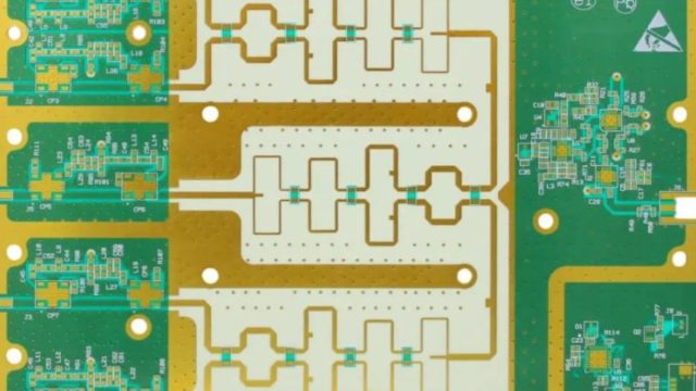
Design Considerations for RF Test PCB
Effective RF Test PCB design requires careful attention to:
-
Short RF signal paths
-
Optimized ground structure and via fencing
-
Minimized discontinuities and stubs
-
Proper RF shielding and isolation
-
Connector launch optimization
Close coordination between RF design and PCB manufacturing is critical.
Manufacturing Challenges of RF Test PCB
Manufacturing an RF Test PCB requires advanced process control:
-
Tight impedance tolerance (±5% or better)
-
Fine line and spacing accuracy
-
Copper surface roughness control
-
Precise layer alignment
-
Impedance and electrical testing
Any process variation can affect RF test accuracy.
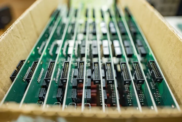
Advantages of Professional RF Test PCB Manufacturing
Working with an experienced RF Test PCB manufacturer provides:
-
Accurate and repeatable RF performance
-
Stable impedance and low insertion loss
-
Support for high-frequency and mmWave testing
-
Reliable quality for prototype and production test boards
-
Faster RF validation cycles
These advantages are critical for RF testing environments.
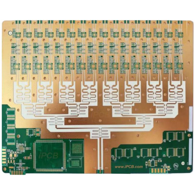
Applications of RF Test PCB
RF Test PCBs are widely used in:
-
RF module and chipset testing
-
5G and mmWave device validation
-
Wireless communication equipment testing
-
Semiconductor ATE and load boards
-
Radar and RF sensor evaluation
-
Production test fixtures
They are essential tools throughout the RF product lifecycle.
Conclusion
An RF Test PCB is a key component in accurate RF measurement and validation. By combining low-loss materials, precise impedance control, and controlled manufacturing processes, RF Test PCBs ensure reliable and repeatable RF test results.
Choosing a qualified RF Test PCB manufacturer guarantees high-frequency performance, measurement accuracy, and long-term reliability for RF testing applications.
