With the rapid advancement of RF and wireless semiconductor devices, precise testing at high frequencies has become critical. An RF IC Test PCB provides the necessary electrical interface for high-frequency ICs during automated test equipment (ATE) validation, ensuring accurate signal transmission, impedance matching, and repeatable test results.
RF IC test PCBs are widely used in wireless communications, 5G modules, RF transceivers, and other high-frequency semiconductor applications.
What Is an RF IC Test PCB?
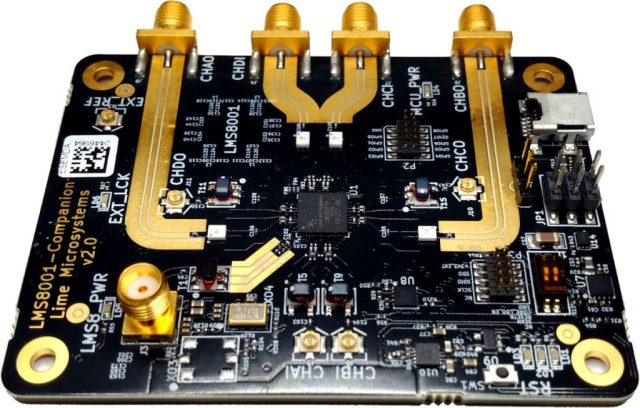
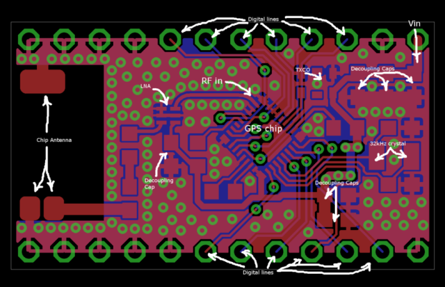
An RF IC Test PCB is a specialized printed circuit board designed to test high-frequency integrated circuits. Unlike standard IC test PCBs, RF IC test PCBs must handle GHz-level signals with minimal signal loss, controlled impedance, and minimal crosstalk.
These boards often serve as load boards, probe card interfaces, or custom test fixtures in ATE systems for RF chip testing.
Key Requirements for RF IC Test PCBs
High-Frequency Signal Integrity
RF IC test PCBs must maintain low-loss, high-speed signal paths to ensure accurate measurement at GHz frequencies.
Controlled Impedance
Precise impedance control is critical to reduce reflection, signal distortion, and insertion loss in RF testing.
High Pin Count
Modern RF ICs often have many signal, power, and ground pins. Dense routing and multilayer designs are essential to accommodate high pin counts.
Thermal and Mechanical Stability
High-frequency testing may generate heat; RF IC test PCBs must withstand thermal cycling and repeated probe contact without degradation.
RF IC Test PCB Design Considerations
Effective RF IC test PCB design includes:
-
Optimized multilayer stack-up with signal, ground, and power layers
-
Controlled impedance routing and trace width optimization
-
Differential pair and length-matched routing for high-frequency signals
-
Low-loss materials suitable for GHz-level testing
-
Careful placement of connectors, sockets, and probe interfaces
Close collaboration with RF test engineers ensures reliable high-frequency performance.
Materials Used in RF IC Test PCBs
RF IC test PCBs commonly use:
-
Low-loss laminates such as Rogers RO4350B, RO4003C, or RF-35
-
High-Tg FR-4 for mixed-signal RF boards
-
Advanced prepregs for consistent dielectric thickness
Material selection ensures minimal signal attenuation and stable impedance at high frequencies.
Manufacturing Capabilities for RF IC Test PCBs
Fabrication of RF IC test PCBs requires:
-
Fine line and spacing control
-
Multilayer PCB and HDI capabilities
-
Blind and buried vias for dense layouts
-
Impedance testing and validation
-
Strict thickness and material tolerance control
Advanced manufacturing ensures RF performance meets stringent specifications.
RF IC Test PCB Assembly Services
Assembly for RF IC test PCBs may include:
-
High pin count socket and connector installation
-
Fine-pitch SMT component assembly
-
Mixed SMT and through-hole assembly
-
X-ray inspection for hidden solder joints
Proper assembly maintains signal integrity and mechanical reliability during testing.
Applications of RF IC Test PCBs
RF IC test PCBs are commonly used in:
-
5G RF IC testing and validation
-
Wi-Fi, Bluetooth, and other wireless IC testing
-
RF transceiver module evaluation
-
High-frequency mixed-signal IC testing
-
Semiconductor wafer and final package testing
These applications demand precise impedance control and high-frequency signal fidelity.
Prototype and Small Batch RF IC Test PCBs
Prototype or small batch RF IC test PCBs are critical for early-stage validation, design verification, and test program development. Rapid turnaround and engineering support help reduce development time and improve measurement accuracy.
Small batch production also allows optimization of layout, stack-up, and materials before scaling to full production.
Why Choose a Specialized RF IC Test PCB Manufacturer?
A professional RF IC test PCB manufacturer provides:
-
Expertise in high-frequency PCB design and fabrication
-
Precision manufacturing with controlled impedance verification
-
Support for high pin count and multilayer RF designs
-
Flexible volumes from prototype to production
This ensures RF IC test PCBs deliver reliable, repeatable, and accurate high-frequency performance.
Conclusion
RF IC Test PCB manufacturing is essential for accurate and reliable high-frequency semiconductor testing. With optimized materials, precise impedance control, and advanced fabrication techniques, RF IC test PCBs ensure stable signal integrity, accurate measurements, and efficient RF device validation.
Partnering with an experienced RF IC test PCB supplier accelerates development and ensures consistent high-frequency test results.
