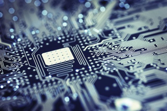
With the rapid advancement of 5G, IoT, Wi-Fi, and mmWave technologies, RF integrated circuits (RF ICs) are becoming increasingly complex and high-speed. Ensuring accurate characterization and validation of these devices requires specialized RF IC Test PCBs capable of maintaining signal integrity at high frequencies.
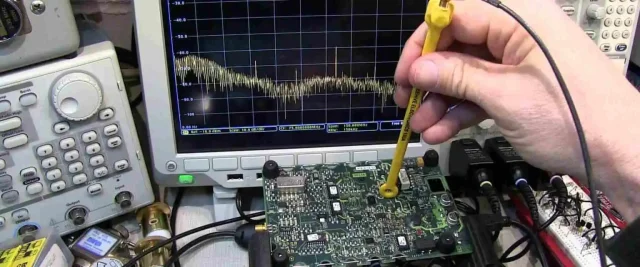
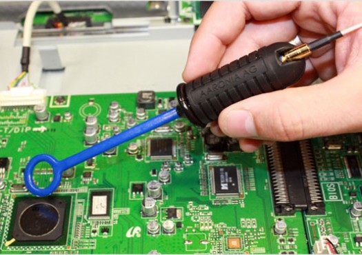
A well-designed RF IC Test PCB serves as the critical interface between RF chips and automated test equipment (ATE), enabling precise functional testing, parametric measurement, and wafer-level RF performance validation.
What Is an RF IC Test PCB?
An RF IC Test PCB is a high-performance printed circuit board specifically engineered for testing RF and wireless semiconductor devices. It connects RF ICs to ATE systems, probe cards, or test sockets while preserving signal integrity at high frequencies.
Key functions include:
-
High-frequency signal routing between RF ICs and test instruments
-
Controlled impedance for RF and microwave signals
-
Low insertion loss and reduced signal reflections
-
Mechanical precision for probe alignment and stable testing
RF IC test PCBs are designed to deliver accuracy, repeatability, and reliability in demanding RF test environments.
Key Features of RF IC Test PCBs
-
Controlled Impedance for RF Signals
Ensures stable transmission of RF signals and accurate S-parameter and performance measurements. -
Low-Loss High-Frequency Routing
Minimizes attenuation and distortion at GHz and mmWave frequencies. -
High-Density and High Pin Count Design
Supports modern RF ICs with fine-pitch pads and complex I/O configurations. -
Multilayer and HDI Stackups
Optimized layer structures improve isolation between RF, digital, power, and ground signals. -
Mechanical Precision and Stability
Maintains accurate probe or socket alignment during repeated RF test cycles.
Materials and Stackup Considerations
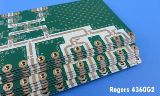
Material selection is critical for RF IC Test PCB performance:
-
Low-Loss RF Laminates (Rogers, Taconic RF-35, Duroid 5880/6002) for high-frequency signal integrity
-
High-Tg FR-4 for mixed RF and digital test designs
-
Hybrid Stackups combining RF materials and FR-4 for cost and performance optimization
-
Thermally Stable Materials to prevent warpage during extended RF testing
Proper materials and stackup design ensure low loss, stable impedance, and repeatable RF measurements.
Applications of RF IC Test PCBs
RF IC test PCBs are widely used in:
-
RF and wireless IC functional and parametric testing
-
5G, Wi-Fi, Bluetooth, and mmWave chip validation
-
Wafer-level RF probing and package-level testing
-
ATE systems, probe cards, and RF load boards
-
Prototype development and small-batch RF IC verification
These applications demand high-frequency accuracy, low noise, and consistent performance, all enabled by professional RF IC test PCB solutions.
Choosing an RF IC Test PCB Manufacturer
When selecting an RF IC Test PCB supplier, key considerations include:
-
Proven experience in high-frequency and RF PCB manufacturing
-
Expertise in controlled impedance and low-loss material processing
-
Capability for multilayer, HDI, and high-pin-count PCBs
-
Support for prototype, small-batch, and volume production
-
Strong engineering support and RF quality control processes
An experienced manufacturer ensures accurate RF testing, reduced development risk, and faster product validation.
Conclusion
RF IC Test PCBs are essential for validating high-frequency and wireless semiconductor devices, providing controlled impedance, low-loss routing, high-density interconnects, and mechanical precision. Whether for 5G, IoT, or microwave applications, a high-quality RF IC test PCB enables accurate measurements, reliable testing, and efficient transition from R&D to mass production.
