Harsh-environment communication terminals—used in battlefield radios, mining telemetry units, emergency response networks, and remote industrial gateways—depend on mmWave Module PCB architectures that can preserve signal integrity, impedance accuracy, and structural reliability under extreme stress. High-frequency circuits operating from 24 GHz to 71 GHz experience sensitivity far greater than conventional RF PCB designs, making material stability, mechanical robustness, and loss control the primary engineering pillars.
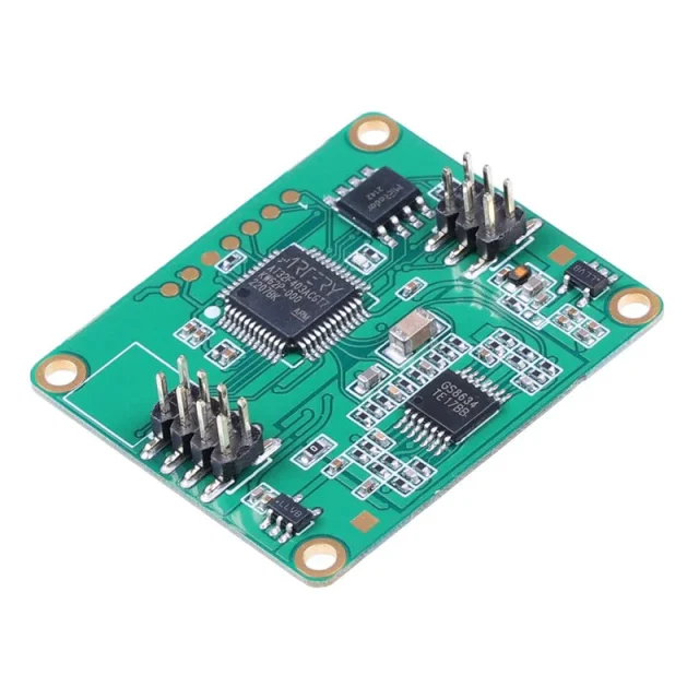
A ruggedized mmWave Module PCB must withstand vibration, impact shock, rapid thermal transitions, humidity cycling, and long-duration RF power exposure without degrading insertion loss or shifting impedance windows. This combination of high-frequency performance and mechanical endurance defines the engineering core of next-generation communication terminals.
1. High-Frequency Integrity: The Central Constraint of mmWave PCB Design
mmWave signals exhibit tight tolerances due to their short wavelengths. Even minor dielectric inconsistencies or conductor imperfections can create dramatic variations in channel performance. Therefore, the PCB must ensure:
-
Stable dielectric constant (Dk) to maintain predictable impedance
-
Low dissipation factor (Df) to prevent insertion loss and amplitude distortion
-
Ultra-smooth copper interfaces to reduce conductor loss
-
Ground uniformity and shielding to suppress mode conversion and radiation
Materials commonly used in ruggedized mmWave Module PCB stackups include:
-
RO4350B, RO4835, Teflon-based laminates, Megtron 7, and hybrid PTFE composites
These substrates combine low-loss properties with thermal and mechanical stability, forming the base of harsh-environment RF design.
2. Mechanical Ruggedization: Surviving Shock, Vibration, and Impact
Communication terminals deployed in harsh conditions face:
-
continuous vibration in vehicles, UAVs, and drilling platforms
-
sudden impact shock during drops or collisions
-
chassis flexing from load shifts and mounting pressure
-
temperature swing stress causing microcracks or CTE expansion failures
To combat these, a ruggedized mmWave Module PCB incorporates:
-
Reinforced multilayer bonding systems
– High-temperature resin systems
– Low-CTE dielectric layers
– Anti-delamination adhesives -
Shock-absorbing via structures
– Staggered via grids
– Filled and capped vias for mechanical stability
– Heavy-copper pad anchors to prevent barrel cracking -
Vibration suppression geometry
– Shorter high-frequency interconnects
– Distributed grounding meshes
– Mechanically balanced stackups (symmetrical dielectric layouts)
These measures prevent trace lift-off, via fatigue, and delamination, ensuring the mmWave module remains electrically stable under sustained mechanical stress.
3. EMI Shielding for Wideband Stability
mmWave modules are inherently sensitive to external RF noise and internal coupling. Ruggedized modules intensify shielding strategies to maintain integrity:
-
Segmented ground planes to reduce cavity resonance
-
Continuous via-fence structures forming effective RF barriers
-
Dielectric pockets that confine fields and suppress cross-band interference
-
Metal shielding cans with thermal-relief structures for heat dissipation
This architecture ensures wideband isolation, maintaining clean mmWave channels even when the device operates near high-power RF sources or in electromagnetically noisy environments.
4. Thermal Reliability Under Extreme Operating Conditions
Harsh-environment terminals run under conditions where ambient temperatures may swing from –40°C up to +125°C, impacting:
-
dielectric expansion
-
impedance windows
-
phase stability
-
thermal runaway in power modules
To stabilize performance, ruggedized mmWave Module PCB designs include:
-
High-conductivity thermal vias directly beneath RF mixers and PA chains
-
PTFE-hybrid substrates with low CTE for predictable expansion
-
Embedded copper backplanes to eject heat uniformly across the stack
-
Simulation-driven layout to predict high-loss hotspots before fabrication
The result is low-loss transmission, minimal drift, and improved long-term reliability in fluctuating and high-temperature environments.
5. KKPCB Engineering Perspective
KKPCB develops mmWave Module PCB solutions specifically for harsh-environment communication terminals by integrating:
-
±2% impedance control across multi-band RF channels
-
microwave-grade stackups (4–14 layers) with hybrid RO/Teflon configurations
-
high-reliability via structures optimized for shock and vibration
-
HFSS + Keysight ADS co-simulation for accurate channel prediction
-
controlled copper roughness (Ra <0.9 µm) for low-loss mmWave routing
-
automated CTE-matched lamination cycles for durable multilayers
This engineering workflow supports stable 24–71 GHz operation even in demanding field conditions.
Engineering Summary
Ruggedized mmWave Module PCB designs are essential for communication terminals deployed in shock-intensive, vibration-rich, and thermally extreme environments. By combining low-loss materials, mechanically fortified stackups, precision impedance control, and EMI-shielded routing, engineers can guarantee high-frequency integrity and long-term reliability.
These architectures enable communication terminals to deliver stable, low-noise, wideband mmWave performance—even under conditions that would destroy conventional RF PCB designs.
