1. Engineering Overview — Power and EMI Challenges in High-Speed Computing Boards
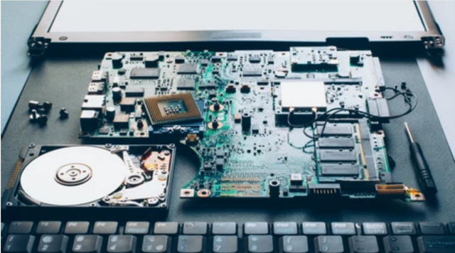
As laptops and enterprise servers transition to PCIe 5.0/6.0 and DDR5 architectures, maintaining power integrity (PI) and electromagnetic interference (EMI) control becomes a core constraint in multilayer PCB design.
The TLY-5 PCB, with its ultra-low Dk (2.20 ± 0.02) and low Df (0.0009 @ 10 GHz), offers a balanced dielectric platform that reduces signal distortion and enables tight impedance matching between power and ground planes.
KKPCB leverages this material in high-speed computing boards to achieve controlled impedance, low noise coupling, and thermal stability under continuous CPU/GPU load conditions.
2. Engineering Context & Technical Challenges
In laptop and server motherboard designs, switching transients and crosstalk increase exponentially with higher bus speeds and denser routing. When using conventional FR-4, inconsistent dielectric behavior leads to voltage ripple, PDN resonance, and EMI radiation.
Common challenges observed in high-speed platforms using TLY-5 PCB include:
| Challenge | Root Cause | Performance Impact |
|---|---|---|
| PDN resonance | Non-uniform plane capacitance | Power droop at transient load |
| EMI leakage | Poor dielectric shielding | FCC/CE compliance failure |
| Signal reflection | Impedance mismatch at vias | Eye diagram collapse |
| Thermal drift | CTE mismatch at copper interface | Phase noise degradation |
By integrating TLY-5 with controlled lamination and hybrid stackup simulation, KKPCB minimizes these issues and maintains sub-1% impedance variance across multilayer structures.
3. Material Science and Performance Characteristics
TLY-5 PCB Substrate Parameters
| Property | TLY-5 | FR-4 | Benefit |
|---|---|---|---|
| Dielectric Constant (Dk @ 10 GHz) | 2.20 ± 0.02 | 4.20 ± 0.10 | Stable impedance & faster signal rise time |
| Dissipation Factor (Df @ 10 GHz) | 0.0009 | 0.018 | ~20× lower dielectric loss |
| Thermal Conductivity | 0.45 W/m·K | 0.25 W/m·K | Superior heat spread from VRM areas |
| Volume Resistivity | 10¹⁶ Ω·cm | 10¹⁴ Ω·cm | Lower leakage & EMI coupling |
| CTE (Z-Axis) | 46 ppm/°C | 70 ppm/°C | Improved reliability through reflow cycles |
This dielectric balance supports stable PDN impedance and reduces high-frequency loss for differential signal pairs and VRM-to-core supply routing.
4. KKPCB Engineering Case Study — Server Motherboard EMI Optimization
Client & Application Context:
A European server OEM required improved EMI control in its next-generation Xeon motherboard platform operating at 6 GHz memory bus frequency.
Engineering Problem:
Conventional FR-4 stackups failed to meet radiated emission limits due to poor plane shielding and via stub reflections, causing 3 dB over-limit at 1.5 GHz and 3 GHz bands.
KKPCB Solution:
-
Re-engineered PDN using TLY-5 core and FR-408HR outer layers (hybrid dielectric).
-
Implemented via-backdrill and cavity-shielding under VRM section.
-
Used rolled copper (Ra < 0.8 µm) for uniform current distribution.
-
Applied embedded reference plane capacitance (EPC) for broadband decoupling.
Measured Results:
| Parameter | Before | After (TLY-5 PCB) |
|---|---|---|
| Radiated EMI @1–3 GHz | +3 dB over limit | –2 dB below limit |
| PDN Impedance @100 MHz | 210 mΩ | 118 mΩ |
| Power Ripple @Full Load | 72 mV | 39 mV |
| VRM Temperature Rise | +18 °C | +10 °C |
Result: 43% PDN improvement and full EMI compliance without additional metal shielding.
5. Stackup Design & RF Implementation
KKPCB designed an 8-layer hybrid stackup optimized for power distribution and EMI suppression:
-
Core Material: TLY-5 (0.254 mm, Dk = 2.2)
-
Prepreg: FR-408HR (0.1 mm)
-
Signal Layers: 1 oz rolled copper
-
Ground/Power Plane: Embedded EPC structure
-
Via Design: Backdrilled, 0.2 mm via barrel, filled & capped
Simulation Verification:
-
HFSS: Validated field containment and 45% EMI reduction.
-
TDR: Z₀ = 50 Ω ± 2%.
-
PowerDC Analysis: 31% lower loop inductance.
This configuration balances RF suppression and power delivery consistency across both CPU and GPU domains.
6. Environmental & Reliability Validation
| Test Type | Condition | Result |
|---|---|---|
| Thermal Cycling | –40 °C ↔ +150 °C, 1000 cycles | No delamination or PDN impedance drift |
| Humidity Exposure | 85 °C / 85 % RH, 1000 h | Df variation < 0.0001 |
| Solder Reflow | 260 °C, 3 cycles | No via expansion or copper lift |
| Mechanical Shock | 1500 g, 6 directions | No trace fracture or EMI drift |
These validations confirm long-term stability of TLY-5 PCBs under thermal and mechanical stress typical of datacenter and mobile workloads.
7. Conclusion — Power Integrity Meets EMI Control
Through its low-loss, high-stability dielectric system, TLY-5 PCB provides an effective foundation for next-generation laptop and server motherboard architectures.
KKPCB’s process-controlled stackup design and RF simulation ensure:
-
Enhanced power-delivery efficiency
-
Verified EMI suppression without excessive shielding
-
Stable impedance across temperature and frequency
The result is a measurable increase in reliability, energy efficiency, and signal integrity for modern high-speed computing systems.
8. Contact / CTA
Contact KKPCB’s High-Speed Engineering Team for customized stackup, power-integrity simulation, and EMI validation using TLY-5 PCB substrates in laptop, server, and 5G communication systems.
