As semiconductor devices continue to scale down while pin counts and test speeds increase, wafer-level testing has become more demanding than ever. At the center of this process is the probe card PCB, a precision-engineered substrate that ensures accurate electrical connection between automated test equipment (ATE) and semiconductor wafers.
A well-designed probe card PCB is critical to maintaining test accuracy, yield stability, and long probe card service life.
The Function of a Probe Card PCB in Wafer Testing
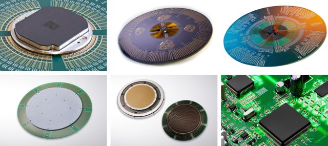
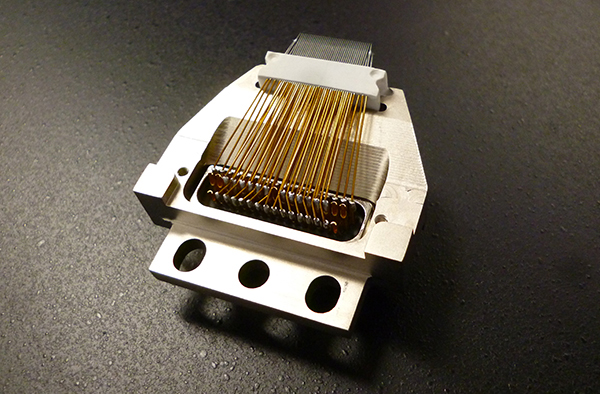
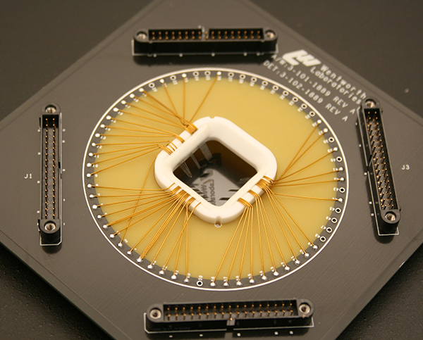
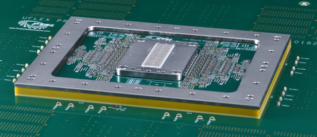
A probe card PCB serves as the electrical backbone of the probe card assembly. It routes power, control, and high-speed signals between probe elements and the ATE system.
Unlike standard PCBs, probe card PCBs must deliver:
-
Extremely consistent electrical paths
-
Support for thousands of simultaneous signal channels
-
Stable performance under repeated probe touchdowns
-
Precise mechanical alignment
Any inconsistency can directly affect wafer test results.
Challenges Driven by High Pin Count and Fine Pitch
Modern ICs require probe card PCBs that can support:
-
Ultra-fine pitch routing
-
High-density interconnect (HDI) structures
-
Multilayer stackups for signal separation
As pin counts increase, maintaining uniform impedance and minimizing crosstalk becomes a major design and manufacturing challenge.
Signal Integrity Requirements in Probe Card PCBs
High-speed wafer testing demands excellent signal integrity. Probe card PCB design must address:
-
Controlled impedance routing
-
Short and symmetrical signal paths
-
Robust ground referencing
-
Isolation of sensitive analog and high-speed digital signals
Consistent signal behavior across all channels ensures reliable test measurements.
Mechanical Stability and Flatness Control
Probe card PCBs experience continuous mechanical stress from probing cycles. Critical requirements include:
-
Excellent PCB flatness
-
Minimal warpage over temperature
-
Reinforced regions for probe attachment
Mechanical stability directly affects probe contact accuracy and wear consistency.
Materials Used for Probe Card PCBs
Material selection balances electrical and mechanical needs. Common choices include:
-
High-Tg FR-4 for structural rigidity
-
Low-loss laminates for high-speed signal paths
-
Low-CTE materials to maintain dimensional stability
Stable materials help ensure consistent performance over long test cycles.
Manufacturing Precision for Probe Card PCBs
Producing a reliable probe card PCB requires advanced fabrication control:
-
Fine-line etching accuracy
-
Tight drilling and via plating tolerances
-
Precise layer alignment
-
Clean manufacturing environments to avoid contamination
Manufacturing consistency is essential for repeatable test results.
Quality Control and Validation
Professional probe card PCB manufacturers implement:
-
Electrical continuity and impedance testing
-
Dimensional and flatness inspection
-
Process traceability for repeat builds
These measures ensure that each probe card PCB performs predictably in production testing.
Applications of Probe Card PCBs
Probe card PCBs are widely used in:
-
Logic and processor wafer testing
-
Memory device testing
-
Mixed-signal and analog IC validation
-
RF and high-speed semiconductor devices
Each application places strict demands on precision and repeatability.
Selecting the Right Probe Card PCB Manufacturing Partner
When choosing a probe card PCB supplier, consider:
-
Experience with semiconductor test PCBs
-
HDI and fine-pitch manufacturing capability
-
Controlled impedance expertise
-
Proven consistency across production runs
A reliable partner helps maintain yield and reduce test downtime.
Conclusion
The probe card PCB is a critical component in modern wafer-level testing, enabling high-pin-count connectivity, stable signal integrity, and long-term mechanical reliability. Through precision design, advanced materials, and tightly controlled manufacturing processes, high-quality probe card PCBs support accurate, repeatable semiconductor testing at scale.
Choosing the right probe card PCB manufacturing partner ensures stable test performance, higher yield, and longer probe card lifespan.
