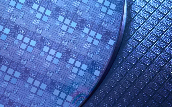
As semiconductor nodes continue to shrink and pin counts rise, the performance of probe cards becomes increasingly critical. Probe Card PCB Assembly is a highly specialized process that combines precision PCB fabrication, accurate component assembly, and strict quality control to ensure reliable wafer-level testing.
A well-executed probe card PCB assembly directly impacts test accuracy, yield, and long-term reliability in semiconductor manufacturing.
What Is Probe Card PCB Assembly?
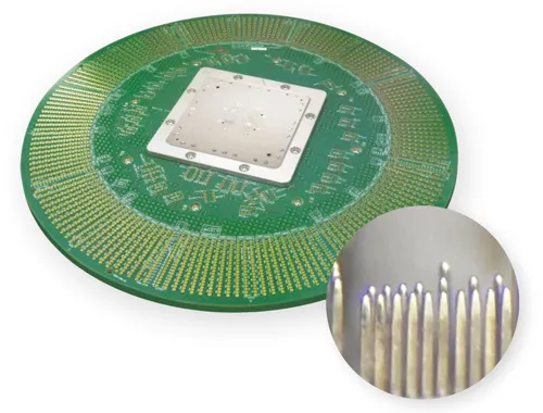
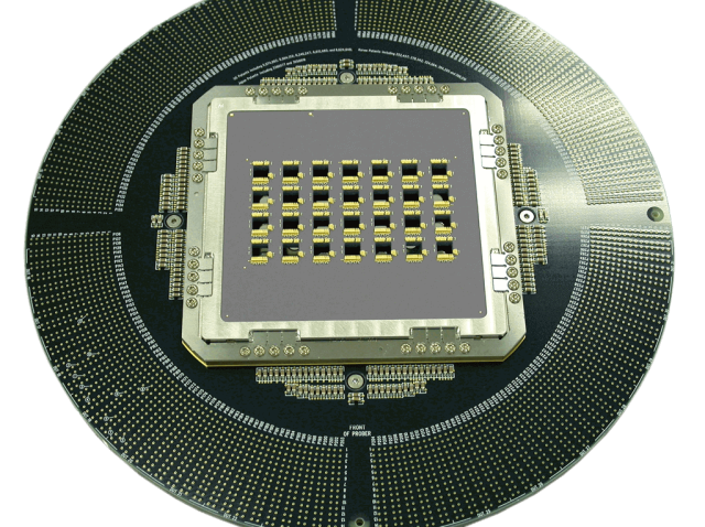
Probe card PCB assembly refers to the process of assembling electronic components and interconnect structures onto the PCB used in wafer probe cards. These PCBs serve as the electrical interface between the wafer under test and automated test equipment (ATE).
Key roles include:
-
Routing high-density signals from probes to ATE channels
-
Providing stable power and ground distribution
-
Maintaining controlled impedance for high-speed signals
-
Ensuring mechanical precision for probe alignment
Key Requirements for Probe Card PCB Assembly
To meet demanding wafer test conditions, probe card PCB assembly must address several critical factors:
-
High Pin Count Support
Probe card PCBs often feature extremely high pin counts, requiring fine-pitch assembly and advanced multilayer designs. -
Controlled Impedance and Signal Integrity
Accurate impedance control minimizes signal reflection and crosstalk, ensuring clean measurement results during high-speed testing. -
Mechanical Accuracy and Stability
Precise component placement and flatness are essential to maintain probe-to-pad alignment across repeated test cycles. -
Thermal Reliability
Stable assembly performance under thermal stress prevents signal drift and mechanical deformation during extended wafer testing.
Materials and Stackup Considerations
Probe card PCB assemblies typically use:
-
High-Tg FR-4 for standard wafer testing
-
Low-loss materials for high-frequency or RF probe cards
-
Hybrid stackups to balance electrical performance and cost
Proper material selection enhances both electrical reliability and mechanical durability.
Applications of Probe Card PCB Assembly
Probe card PCB assembly is widely used in:
-
Wafer-level functional and parametric testing
-
High-speed and mixed-signal semiconductor testing
-
Advanced logic, memory, and RF IC validation
-
ATE probe card interfaces
These applications demand consistent performance across thousands of probe touchdowns.
Choosing a Probe Card PCB Assembly Partner
When selecting a probe card PCB assembly supplier, consider:
-
Experience with semiconductor test PCBs and probe card designs
-
Capability for high pin count, fine-pitch, and multilayer assembly
-
Strict quality control and electrical testing processes
-
Support for prototype, small batch, and volume assembly
A reliable partner ensures precision, repeatability, and long-term test stability.
Conclusion
Probe Card PCB Assembly is a critical element in semiconductor wafer testing, requiring exceptional precision, controlled impedance, and mechanical reliability. By combining advanced PCB manufacturing with accurate assembly processes, probe card PCB assemblies enable high-yield, repeatable, and reliable IC testing.
Partnering with an experienced probe card PCB assembly manufacturer ensures stable performance from early validation through high-volume semiconductor production.
