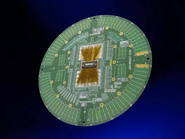
As semiconductor devices continue to scale toward higher speed, higher density, and smaller geometries, wafer-level testing demands extremely precise and reliable interconnection solutions. Probe Card Assembly PCBs play a critical role in automated test equipment (ATE) systems, enabling accurate electrical contact between test instruments and semiconductor wafers during IC, memory, logic, and RF chip testing.
A high-quality probe card assembly PCB must meet strict electrical, mechanical, and dimensional requirements to ensure consistent signal integrity, repeatable contact force, and long service life throughout high-cycle testing environments.
Key Requirements of Probe Card Assembly PCBs
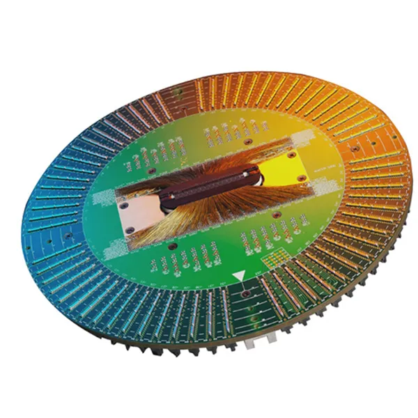
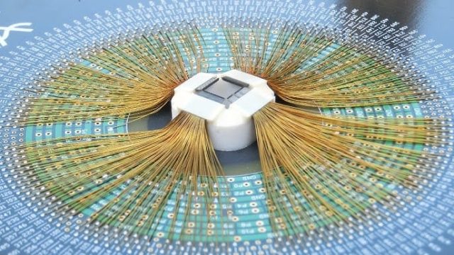
Probe Card Assembly PCBs are far more complex than standard PCBs. They are engineered specifically for semiconductor testing applications and must support:
-
Ultra-high pin count and fine pitch layouts
-
High-density routing and microvia technology
-
Controlled impedance for high-speed and RF signal paths
-
Excellent flatness and tight mechanical tolerances
-
Low loss and low noise performance
These requirements are essential to maintain signal accuracy during wafer probing, especially for high-frequency, high-speed, and mixed-signal devices.
Advanced PCB Technologies for Probe Card Assembly
To meet the demanding needs of probe card applications, advanced PCB manufacturing technologies are required, including:
-
HDI PCB structures with stacked or staggered microvias
-
Multilayer constructions for complex signal and power routing
-
Fine line / fine space capability for dense probe layouts
-
Specialized surface finishes to support probe contact reliability
-
Hybrid stackups for RF IC and high-speed digital testing
These technologies ensure stable electrical performance while supporting the mechanical precision required for probe alignment and repeated probing cycles.
Materials for Probe Card Assembly PCB
Material selection directly impacts the performance and durability of probe card PCBs. Common materials include:
-
High-Tg FR-4 for general IC and logic testing
-
Low-loss laminates for high-speed and RF probe card applications
-
Hybrid material stackups for mixed-signal and microwave IC testing
Low Dk and low Df materials help minimize signal attenuation and timing skew, which is critical for advanced node semiconductor testing.
Applications of Probe Card Assembly PCBs
Probe Card Assembly PCBs are widely used in:
-
Wafer-level IC testing
-
Memory and DRAM wafer probing
-
RF IC and mmWave chip testing
-
Logic and processor wafer validation
-
Semiconductor R&D and engineering verification
They are an essential component of semiconductor manufacturing lines, supporting both high-volume production testing and engineering development.
Why Choose a Professional Probe Card Assembly PCB Manufacturer
Manufacturing probe card assembly PCBs requires deep experience in semiconductor test requirements, precision PCB fabrication, and strict quality control. A reliable PCB partner can provide:
-
Engineering support for complex probe card designs
-
Tight tolerance fabrication and inspection
-
Small batch and prototype capability for test development
-
Stable quality for long-term production programs
Professional probe card PCB manufacturers help ensure accurate testing, reduced downtime, and improved yield across the semiconductor testing process.
