Why PCB Pad Soldering Process Matters
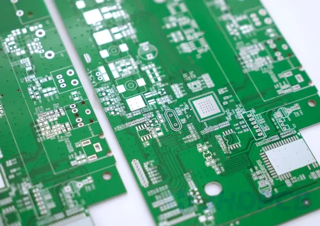
In PCB manufacturing, the pad surface finish or soldering process directly affects component solderability, electrical performance, and long-term reliability.
Different processes offer varying degrees of oxidation resistance, flatness, and cost efficiency, making proper selection essential for every PCB design project.
This article categorizes and compares the most common PCB pad soldering processes, explaining how to choose the right one for your product.
1. Classification by Surface Treatment Process
1.1 Hot Air Solder Leveling (HASL)
Principle: The PCB is immersed in molten tin-lead or lead-free solder, and hot air knives remove excess solder, leveling the surface.
Features:
-
Mature and low-cost process
-
Thick solder coating and good solderability
-
Poor surface flatness — unsuitable for fine-pitch components
-
Lead-free HASL has slightly reduced solderability
Applications:
Low-end consumer electronics, industrial control boards, and general-purpose PCBs.
1.2 Electroless Nickel Immersion Gold (ENIG)
Principle: Copper pads are plated first with nickel, then with a thin gold layer.
Features:
-
Excellent flatness for fine-pitch and BGA components
-
Oxidation-resistant and stable contact resistance
-
Higher cost; potential risk of “black pad” formation in poor processes
Applications:
Smartphones, high-speed communication devices, computer motherboards, and aerospace electronics.
1.3 Immersion Silver (ImAg)
Principle: Silver is chemically deposited onto copper pads via a displacement reaction.
Features:
-
Smooth surface and excellent solderability
-
Moderate cost, but silver easily oxidizes
-
Risk of silver migration under high humidity
Applications:
Medium-precision digital circuits, automotive electronics, and telecommunication boards.
1.4 Immersion Tin (ImSn)
Principle: Tin is deposited on copper pads through a chemical displacement process.
Features:
-
Fine surface finish and good solderability
-
Environmentally friendly, lead-free alternative to HASL
-
Thin and soft tin layer—easily scratched or damaged
Applications:
Consumer electronics, home appliances, and mid-range PCBs.
1.5 Hard Gold Plating
Principle: Uses electrolytic plating to deposit a hard gold alloy layer with cobalt or nickel.
Features:
-
Very high hardness and wear resistance
-
Excellent durability for repeated insertions
-
Expensive process
Applications:
Connectors, keypads, gold fingers, and edge connectors.
1.6 Organic Solderability Preservative (OSP)
Principle: A thin organic coating is applied to copper pads to prevent oxidation before soldering.
Features:
-
Very low cost and eco-friendly
-
Smooth and flat surface
-
Short shelf life; not suitable for multiple reflows
Applications:
High-density, low-cost consumer electronics and disposable devices.
1.7 Electroless Nickel Electroless Palladium Immersion Gold (ENEPIG)
Principle: Sequential deposition of nickel, palladium, and gold layers.
Features:
-
Superior corrosion resistance
-
Excellent wire bonding and soldering performance
-
High cost, but extremely reliable
Applications:
Automotive electronics, aerospace systems, and high-reliability defense or medical PCBs.
2. Classification by Pad Shape and Function
| Pad Type | Function | Typical Surface Treatment |
|---|---|---|
| Standard Solder Pads | Component soldering interface | HASL, ENIG, or OSP |
| Via Pads | Electrical interconnection, sometimes for soldering | HASL or ENIG |
| Thermal Pads | Heat dissipation for power components | HASL or ENIG with thermal vias |
| Gold Fingers | Edge connector contacts | Hard gold plating |
3. Process Comparison Summary
| Process | Solderability | Flatness | Cost | Durability | Applications |
|---|---|---|---|---|---|
| HASL | ★★★★★ | ★★☆☆☆ | ★★☆☆☆ | ★★★☆☆ | General electronics |
| ENIG | ★★★★★ | ★★★★★ | ★★★★☆ | ★★★★☆ | High-end fine-pitch PCBs |
| OSP | ★★★★☆ | ★★★★★ | ★☆☆☆☆ | ★★☆☆☆ | High-density, low-cost |
| ImAg | ★★★★★ | ★★★★★ | ★★☆☆☆ | ★★★☆☆ | Medium-precision circuits |
| ImSn | ★★★★☆ | ★★★★★ | ★★☆☆☆ | ★★☆☆☆ | Lead-free consumer electronics |
| Hard Gold | ★★★☆☆ | ★★★☆☆ | ★★★★★ | ★★★★★ | Connectors, gold fingers |
| ENEPIG | ★★★★★ | ★★★★★ | ★★★★★ | ★★★★★ | High-reliability aerospace & automotive |
4. PCB Surface Finish Selection Guide
For cost-sensitive, large-pitch PCBs: Choose HASL or OSP
For fine-pitch and high-reliability designs: Choose ENIG or ENEPIG
For connectors and wear-resistant areas: Choose Hard Gold Plating
For moderate-cost and mid-performance boards: Choose Immersion Silver
For lead-free and RoHS-compliant applications: Choose Immersion Tin
Your choice should balance product cost, assembly reliability, and application environment.
Matching Process to Performance
Selecting the right PCB pad soldering process is key to ensuring solder reliability, long-term performance, and manufacturing yield.
By understanding the advantages and limitations of each finish—HASL, ENIG, OSP, ImAg, ImSn, Hard Gold, and ENEPIG—designers and manufacturers can choose the most cost-effective solution for each project.
