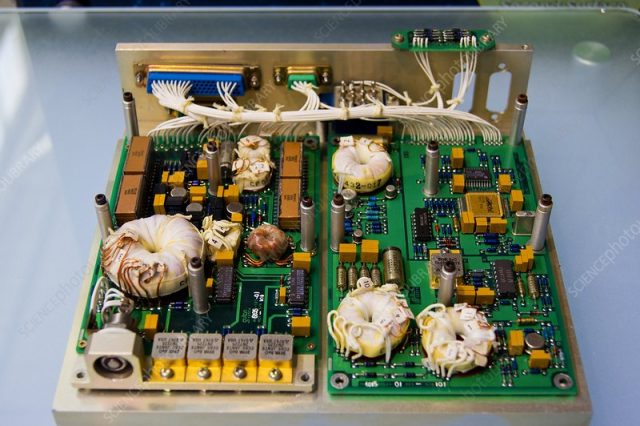
LEO constellation terminals—whether phased-array user antennas, gateway stations, or compact mobile terminals—are being pushed toward wideband RF performance, higher transmit power, and increasingly integrated architectures.
This raises a persistent engineering challenge: how to maintain thermal reliability inside a multilayer high-density PCB where RF, digital, and power systems coexist in tight proximity.
At orbital altitudes, temperature swings are brutal and frequency-specific behavior becomes even more sensitive. A PCB stackup that cannot stabilize heat flow will suffer impedance drift, phase deviation, interlayer warpage, and eventual RF link degradation.
High-density satellite PCB stackups engineered by KKPCB solve these issues through low-Df materials, controlled-CTE bonding systems, and thermal-guided layer architectures optimized for LEO terminal duty cycles.
Thermal Challenges Unique to LEO Constellation Hardware
LEO constellations produce a different thermal profile than GEO or MEO systems. The PCB must endure:
• Rapid temperature transitions from –140°C to +120°C
• Long-duration RF transmission at Ka- / Ku- / X-band
• Compact antennas forcing high interlayer density
• Aggressive power amplifiers with localized hotspots
• Continuous beamforming requiring phase coherence
Conventional PCB stackups cannot maintain predictable electrical and mechanical behavior under these conditions. Thermal fatigue compounds until micro-via interfaces, RF feed networks, or ground planes exhibit drift or cracking.
Material Science: Selecting Laminates with True Thermal Discipline
KKPCB engineers select satellite-grade laminates built for high-frequency and thermal endurance. Typical combinations include:
• RO4835 / RO3003 / RO5880 for low Df transmission (Df 0.001–0.003)
• Low-CTE bonding films to stabilize expansion across layers
• High-conductivity copper planes to distribute PA heat
• Ceramic-filled hydrocarbon substrates for minimal dielectric shift under temperature
These materials preserve Dk/Df consistency, preventing RF degradation even under extreme heating and cooling cycles.
High-Density Stackup Engineering for Thermal Reliability
A thermally reliable satellite PCB is fundamentally a stackup problem.
KKPCB deploys the following architectural principles:
Thermal-Layer Zoning
Different functional zones—RF, PA power, control logic—are isolated by layers tuned for their thermal and electrical requirements.
This prevents high-power RF amplifiers from bleeding heat into sensitive low-noise circuitry.
Distributed Copper Heat Spreading
Thick copper planes and hybrid micro-via arrays redirect heat away from hotspots.
Thermal vias aligned under PA devices create a vertical heat-escape path into the system’s mechanical heat spreaders.
CTE-Balanced Multilayer Alignment
Carefully selected films and laminates minimize warpage across 10–20 layers, ensuring long-term phase stability and structural reliability.
Low-Loss RF Routing Strategy
Microstrip / stripline routing is optimized to maintain low insertion loss even when temperature fluctuates.
This is crucial for LEO terminals where beam tracking and pointing accuracy rely on phase integrity.
Case Implementation: High-Density LEO Phased-Array User Terminal
A recent KKPCB project involved an 18-layer Ka-band phased-array terminal needing:
• <0.25 dB/in insertion loss at 29 GHz
• Phase deviation <0.7° across heating cycles
• Impedance variation <2.5% across all beamforming paths
• Stable operation during ±125°C thermal cycles
KKPCB Achievements:
• Achieved 0.21 dB/in loss using hybrid RO5880 + low-CTE dielectric stackup
• Phase deviation reduced to 0.48° through matched-expansion stack surgical alignment
• Thermal rise under full TX power lowered by 22% using targeted copper heat planes
• Zero micro-via cracking after 1000 cycles of orbital thermal simulation
This validated the design for long-term orbital use.
Environmental Reliability Testing
KKPCB’s satellite PCB stackups undergo:
• 1000-cycle thermal shock from –150°C to +130°C
• Vacuum outgassing assessment to prevent orbital contamination
• CTE warpage mapping across every lamination stage
• High-power RF burn-in for multi-hour PA stress testing
• Vibration & shock tests per MIL-STD-810
These validations ensure that LEO terminal PCBs retain dimensional stability, RF integrity, and thermal reliability across the mission lifetime.
Conclusion — Thermal Reliability is the Backbone of LEO Performance
Next-generation LEO constellation terminals can only perform reliably when their PCB architecture maintains:
• Stable impedance
• Predictable RF phase behavior
• Consistent thermal dissipation
• Structural integrity across rapid temperature cycles
High-density satellite PCB stackups designed by KKPCB transform these requirements into repeatable, engineerable outcomes.
As LEO systems expand into broadband communications, autonomous platforms, and global mobility networks, the need for thermally reliable, multilayer, low-loss PCB systems becomes non-negotiable.
KKPCB supports complete engineering—from stackup simulation to environmental qualification—to ensure your spacecraft or ground terminal maintains performance across every orbit.
