Next-generation UAV systems—whether used for industrial IoT sensing, long-range inspection, autonomous mapping, or precision agriculture—depend on PCB platforms capable of delivering high-frequency RF accuracy, ultra-stable GNSS/GPS reception, multi-band communication reliability, and lightweight HDI construction. As flight durations extend and sensor payloads grow more complex, the PCB becomes the backbone that determines navigation precision, RF sensitivity, and electromagnetic cleanliness.
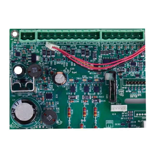
To meet these demands, HDI UAV PCB architectures integrate microvias, low-loss RF dielectrics, controlled-impedance transmission lines, and lightweight multilayer stackups that preserve signal fidelity from GNSS L1 bands to mmWave UAV communication links. The goal is consistent: achieve low-loss routing, low-noise RF front-end stability, and robust EMI suppression, all while keeping weight and thermal load minimized for long-endurance drone missions.
1. RF Signal Integrity Requirements in UAV Navigation Chains
Drone navigation modules rely on combined RF paths, including:
-
GNSS/GPS L1/L5 for global position accuracy
-
Dual-band WiFi / Sub-6 GHz 5G for telemetry
-
mmWave radar or communication links for advanced positioning
-
IMU / sensor fusion buses integrated on the same board
These RF chains demand:
-
Insertion loss reduction across long flex–rigid or multilayer HDI paths
-
Phase stability in wide-temperature outdoor operations
-
Electromagnetic isolation between GNSS receivers, motor ESCs, and RF amplifiers
-
Minimal mode conversion in dense high-frequency routing
-
Stable dielectric constant (Dk) and low dissipation factor (Df) for consistent UAV navigation data accuracy
Low-loss materials such as RO4350B, RO4835, Megtron 6, and LCP-based HF layers ensure the PCB maintains stable RF characteristics even during altitude swings, sun exposure, and vibration-heavy flight cycles.
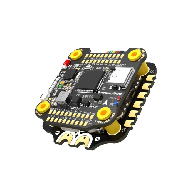
2. Lightweight HDI Construction for Next-Gen Drone Platforms

The shift toward lighter, stronger, and more electrically stable PCB structures drives adoption of:
-
1–3-level HDI microvia structures
-
Stacked and staggered microvias for compact navigation modules
-
Thin dielectric layers (70–100 µm) for controlled RF impedance paths
-
Hybrid stackups combining HF materials + FR-4 cores to reduce weight and cost
-
Rigid–flex integration for folding GNSS antenna boards and sensor wings
This construction reduces mass while improving mechanical stability under vibration. Lightweight HDI UAV PCBs translate directly to improved flight endurance, thermal stability, and navigation precision.
3. RF Routing Architecture for Multi-Band Drone Communication
A UAV navigation PCB must simultaneously support:
-
GNSS front-end LNAs (1.575 / 1.176 GHz)
-
2.4/5.8 GHz UAV telemetry radios
-
High-frequency sensor boards for mmWave altimeters
-
Low-noise IMU and magnetometer interfaces
To avoid desensitization and interference:
-
Microstrip/stripline geometries are optimized using HFSS & ADS
-
RF channels are kept on dedicated low-loss dielectric layers
-
Controlled-impedance lines (50 Ω, 75 Ω, or differential 90–100 Ω) are maintained to ±5%
-
Shielded via fences isolate GNSS receivers from motor driver noise
-
RF transitions through microvias are simulated to minimize discontinuity
This creates a navigation board that maintains clean, high-SNR RF reception even near ESCs, rotors, and switching power supplies.
4. Thermal, Mechanical, and EMI Reliability for UAV Environments
Outdoor UAV missions subject electronics to:
-
Direct sunlight → high thermal gradients
-
Rapid altitude changes → pressure & condensation cycles
-
Mechanical shock → propeller vibration & landing impact
-
High-current motor lines → electromagnetic pollution
To counter these:
-
Thermal vias lower hotspot accumulation in RF amplifiers
-
Low-CTE HF substrates minimize phase drift over temperature
-
Copper roughness control preserves high-frequency insertion loss
-
EMI fences and segmented ground planes suppress cross-domain interference
-
Conformal coating-ready mask designs improve long-term outdoor reliability
The result is a PCB architecture reinforced for near-constant RF stability across harsh UAV operating conditions.
5. KKPCB Engineering Optimization for UAV Navigation PCB Systems
KKPCB implements a full engineering workflow:
-
HFSS multilayer RF simulation of GNSS, 5G, and mmWave transmission
-
Impedance-controlled microvia networks with ±3 μm dielectric precision
-
Hybrid HF stackups balancing weight, Dk/Df stability, and cost
-
High-frequency loss modeling across microstrip–via–module transitions
-
Thermal FEM modeling for ESC and navigation processor hotspots
-
Vibration-grade HDI via reinforcement for UAV shock cycles
-
AOI + TDR validation ensuring routing uniformity for flight-critical signals
This ensures the UAV module maintains low-loss RF propagation, ultra-stable GNSS lock, and high-precision navigation performance in multi-sensor autonomous drone systems.
6. Engineering Summary
Lightweight HDI UAV PCBs—with low-loss RF materials, microvia interconnects, controlled impedance architecture, and multi-band electromagnetic isolation—provide the foundation for high-reliability drone navigation. Optimized PCB engineering enables:
-
Stronger GNSS lock under interference
-
Cleaner RF paths with reduced insertion loss
-
Higher flight endurance through lightweight stackups
-
Stable navigation performance in thermal & vibration extremes
-
Reliable multi-sensor fusion for modern UAV autonomy
KKPCB delivers end-to-end PCB engineering for UAV navigation modules, IoT drone platforms, high-frequency RF chains, and long-range communication systems.
