RF subsystems operating from 10 to 67 GHz—spanning 5G mmWave, satellite links, and aerospace communication modules—demand ultra-stable dielectric properties and minimal signal loss. Any Dk/Df variation or thermal-induced impedance drift directly degrades signal integrity, phase coherence, and overall RF system efficiency.
Duroid 5880 PCB laminates (Dk = 2.2 ± 0.02, Df = 0.0009 @10 GHz) deliver exceptionally low-loss transmission, superior dielectric stability, and predictable impedance across wide bandwidths. KKPCB leverages precision multilayer stackups, low-roughness copper, and advanced lamination techniques to ensure consistent mmWave signal propagation in high-density RF architectures.
Core Engineering Challenges
| Challenge | Root Cause | Engineering Impact |
|---|---|---|
| Dielectric variation across layers | Laminate inconsistency | Impedance mismatch, phase drift |
| High insertion loss at mmWave | Df and copper roughness | Signal attenuation, reduced RF efficiency |
| Thermal-induced deformation | CTE mismatch, high power | Trace misalignment, beamforming errors |
| Crosstalk in dense RF channels | Tight trace spacing, insufficient shielding | Reduced isolation, degraded linearity |
| Phase instability under load | Uneven expansion and dielectric stress | Timing errors, signal distortion |
Material Science – Duroid 5880 Advantages
| Parameter | Typical Value | Engineering Benefit |
|---|---|---|
| Dk | 2.2 ± 0.02 | Predictable impedance for high-frequency RF lines |
| Df | 0.0009 @10 GHz | Ultra-low insertion loss across 10–67 GHz |
| Thermal Conductivity | 0.3 W/m·K | Controlled hotspot dissipation |
| CTE | 16 ppm/°C | Minimal expansion preserves trace alignment |
| Moisture Absorption | 0.02% | Maintains stable dielectric properties under humidity |
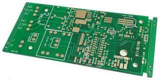
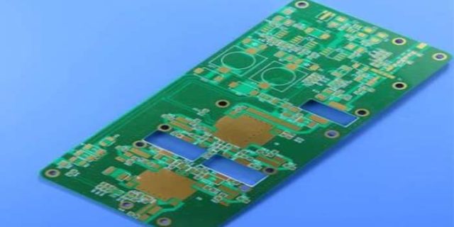
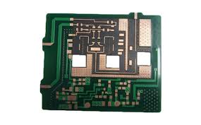
KKPCB Case Study — 10–67 GHz RF Module PCB
Client Context:
A satellite communication vendor required a 6-layer Duroid 5880 PCB supporting high-power RF chains from 10–67 GHz with insertion loss <0.35 dB/in and phase deviation <0.4°.
KKPCB Solution:
-
Precision ±3 µm dielectric thickness control across all layers
-
Smooth copper traces (Ra <0.6 µm) to reduce mmWave loss
-
Segmented ground planes and micro-shielding for EMI suppression
-
Embedded thermal vias and power planes for high-power dissipation
-
HFSS/ADS simulation for phase linearity and impedance verification
Measured Results:
| Parameter | Target | KKPCB Result |
|---|---|---|
| Insertion Loss @28 GHz | <0.35 dB/in | 0.31 dB/in |
| Phase Deviation | <0.4° | 0.37° |
| Thermal Rise | <7°C per layer | 6.3°C |
| EMI Suppression | >30% | 33% |
| Impedance Variation | ±3% | ±1.5% |
Stackup Design & RF Simulation
-
HFSS Modeling: Optimized microstrip/stripline layout for wideband 10–67 GHz
-
ADS & TDR: Phase deviation <0.4° across all RF paths
-
Thermal FEM: Hotspot minimization and uniform temperature distribution
-
AOI & Solder Reflow Monitoring: ±10 µm alignment maintained
Environmental & Reliability Validation
| Test | Condition | Result |
|---|---|---|
| Thermal Cycling | –40°C ↔ +125°C, 1000 cycles | Phase deviation <0.4°, no delamination |
| Vibration & Shock | 5–500 Hz, 10G | No microcracks or solder failures |
| Humidity Testing | 85°C / 85% RH, 1000 h | Stable Dk/Df, phase consistent |
| High-Power RF Operation | Continuous 10–67 GHz | Minimal insertion loss increase (<0.02 dB) |
| Reflow Verification | 260°C ×3 cycles | Stackup alignment maintained |
Engineering Summary & Contact
Duroid 5880 PCB laminates provide ultra-low loss, dielectric stability, and predictable high-frequency behavior for 10–67 GHz RF subsystems. KKPCB’s precision stackup engineering, EMI control, and thermal management ensure high-power RF reliability and wideband phase coherence for 5G, satellite, and aerospace modules.
Contact KKPCB Engineering Team for Duroid 5880 PCB design consultation, multilayer RF stackup optimization, and high-frequency performance validation.
