As semiconductor devices and electronic systems continue to increase in complexity, testing requirements demand higher signal density, better isolation, and improved electrical stability. The Multilayer Test PCB plays a critical role in enabling accurate, repeatable, and high-speed testing across a wide range of applications.
A well-designed multilayer test PCB ensures reliable electrical performance under demanding test conditions.
What Is a Multilayer Test PCB?
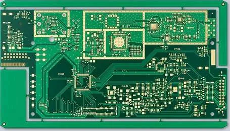
A multilayer test PCB is a specialized printed circuit board consisting of multiple signal, power, and ground layers designed specifically for electrical testing and validation. Compared to simple test boards, multilayer test PCBs support:
-
Dense signal routing
-
Controlled impedance transmission lines
-
Dedicated power and ground planes
These features are essential for high-pin-count and high-speed test environments.
Why Multilayer Test PCBs Are Essential
Modern test systems require:
-
Simultaneous testing of hundreds or thousands of signals
-
Stable power delivery under dynamic loads
-
Low-noise signal transmission
Multilayer test PCBs provide the structural foundation to meet these requirements.
Signal Integrity in Multilayer Test PCB Design
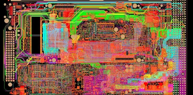
Signal integrity is a primary concern in test boards. Multilayer stackups enable:
-
Shorter signal paths
-
Controlled impedance routing
-
Reduced crosstalk between adjacent signals
Dedicated reference planes improve measurement accuracy.
Power and Ground Plane Optimization
Multilayer test PCBs allow for:
-
Continuous ground planes
-
Low-impedance power distribution
-
Effective decoupling capacitor placement
These design techniques minimize voltage drop and ground bounce during testing.
Layer Stackup and Material Selection
Typical multilayer test PCBs use:
-
High-Tg FR-4 for mechanical stability
-
Low-loss materials for high-speed layers
-
Symmetrical stackups to control warpage
Material selection depends on frequency, signal speed, and test duration.
Via Structures and Interconnect Reliability
Multilayer test PCBs may include:
-
Through-hole vias for robustness
-
Blind and buried vias for dense routing
-
Reinforced via plating for repeated probing
Reliable interconnects are critical for long test cycles.
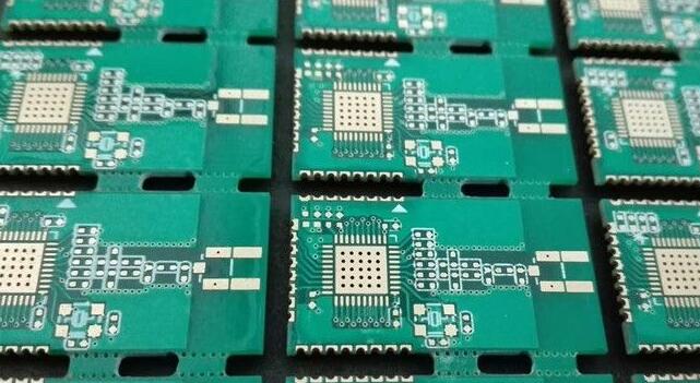
Manufacturing Precision and Quality Control
Manufacturing a multilayer test PCB requires:
-
Tight layer registration control
-
Accurate drilling and plating
-
Electrical and impedance testing
Strict quality control ensures consistent test results.
Typical Applications of Multilayer Test PCBs
Multilayer test PCBs are widely used in:
-
Semiconductor functional and parametric testing
-
ATE systems and evaluation platforms
-
High-speed digital and RF device validation
-
Reliability and stress testing setups
Each application benefits from the scalability of multilayer designs.
Choosing a Multilayer Test PCB Manufacturer
When selecting a multilayer test PCB supplier, consider:
-
Experience with test and measurement PCBs
-
Controlled impedance and stackup expertise
-
Capability for high layer counts
-
Support from prototype to volume production
An experienced manufacturer ensures repeatable and accurate test performance.
Conclusion
The Multilayer Test PCB is a cornerstone of modern electronic and semiconductor testing. By combining dense routing, optimized power distribution, and controlled impedance design, multilayer test PCBs deliver the accuracy and reliability required for advanced testing environments.
Partnering with a professional multilayer test PCB manufacturer ensures stable performance throughout the entire test lifecycle.
