As semiconductor devices and electronic systems continue to increase in speed and complexity, test environments must deliver the same level of precision as the final product. The multilayer test PCB plays a critical role in ensuring accurate measurements, stable signal transmission, and repeatable test results across development and mass production.
A well-designed multilayer test PCB provides the electrical foundation needed for reliable automated testing.
What Is a Multilayer Test PCB?
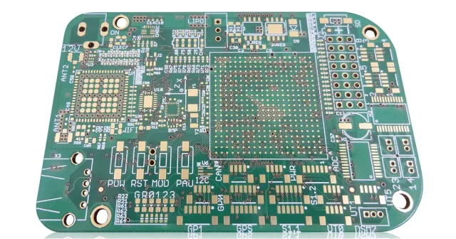
A multilayer test PCB is a specialized printed circuit board built with multiple conductive layers to support complex test requirements. These boards are commonly used in ATE systems, load boards, probe card assemblies, and other semiconductor test platforms.
Key characteristics include:
-
Multiple signal, power, and ground layers
-
Controlled impedance routing
-
High pin-count connectivity
-
Optimized electrical isolation
Multilayer structures allow more complex test functions to be integrated into a compact layout.
Why Multilayer Structure Matters in Test PCBs
Compared with single- or double-layer designs, multilayer test PCBs offer:
-
Better signal isolation and reduced crosstalk
-
Improved power distribution and ground stability
-
Shorter and more controlled signal paths
These advantages are critical for high-speed and high-precision testing environments.
Signal Integrity in Multilayer Test PCB Design
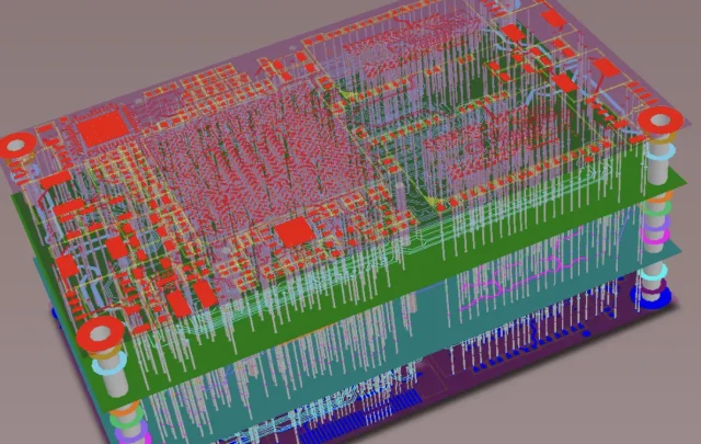
High-speed testing requires stable and predictable signal behavior. Effective multilayer test PCB designs incorporate:
-
Dedicated reference planes for controlled impedance
-
Proper layer pairing for sensitive signals
-
Optimized trace length matching
These design techniques reduce noise and ensure consistent measurements.
Power Integrity and Grounding Strategy
In test systems, power fluctuations can lead to false failures or unstable readings. Multilayer test PCBs support:
-
Low-impedance power planes
-
Robust ground plane structures
-
Effective decoupling capacitor placement
Stable power delivery improves overall test reliability.
Mechanical Stability and Reliability
Multilayer test PCBs must also withstand mechanical and thermal stress caused by:
-
Socket insertion and removal
-
Continuous test cycles
-
Temperature variation
Proper stackup symmetry and material selection help maintain PCB flatness and long-term reliability.
Materials Used in Multilayer Test PCBs
Material choice depends on test requirements:
-
High-Tg FR-4 for structural durability
-
Low-loss laminates for high-speed or RF testing
-
Hybrid stackups for mixed-signal test environments
Stable material properties are essential for consistent electrical performance.
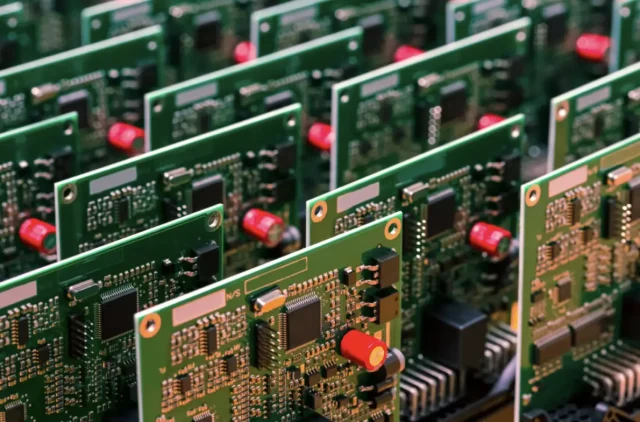
Manufacturing Precision and Consistency
Producing a reliable multilayer test PCB requires strict process control:
-
Accurate layer alignment
-
Uniform copper thickness
-
Reliable via drilling and plating
-
Comprehensive electrical testing
Manufacturing consistency ensures identical performance across multiple test boards.
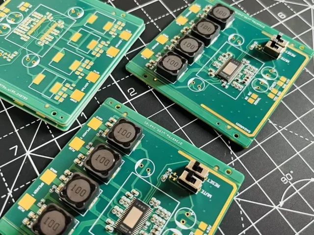
Applications of Multilayer Test PCBs
Multilayer test PCBs are widely used in:
-
Semiconductor ATE systems
-
Load boards and test socket PCBs
-
Probe card assemblies
-
Automotive and industrial electronics testing
Each application benefits from the stability and flexibility of multilayer designs.
Selecting a Multilayer Test PCB Manufacturer
When choosing a multilayer test PCB supplier, look for:
-
Experience with semiconductor test applications
-
Controlled impedance and stackup design expertise
-
Advanced quality inspection capabilities
-
Support for quick-turn and volume production
A reliable partner helps maintain test accuracy and reduce downtime.
Conclusion
The multilayer test PCB is a cornerstone of modern electronic testing systems. By providing superior signal integrity, stable power distribution, and mechanical reliability, multilayer test PCBs enable accurate measurements and consistent test results across high-speed and high-volume environments.
Partnering with an experienced multilayer test PCB manufacturer ensures long-term testing success and higher overall yield.
