What Is a Mixed Signal IC Test PCB?
A Mixed Signal IC Test PCB is a specialized printed circuit board designed for testing mixed-signal integrated circuits that combine analog and digital functions on a single chip. It serves as the interface between the device under test (DUT) and automated test equipment (ATE), enabling accurate measurement of both analog performance and digital functionality.
Mixed signal IC test PCBs are widely used in testing ADCs, DACs, power management ICs, sensor ICs, RF front-end ICs, and other complex semiconductor devices.
Challenges in Mixed Signal IC Testing
Unlike purely digital or analog ICs, mixed signal ICs require test boards that can handle:
-
High-speed digital signals
-
Low-noise analog signals
-
Sensitive power and reference voltages
-
Tight timing and synchronization requirements
A mixed signal IC test PCB must carefully balance signal integrity, noise isolation, and power stability to ensure accurate test results.
Key Requirements for Mixed Signal IC Test PCBs
To meet these challenges, mixed signal IC test PCBs must provide:
-
Controlled impedance routing for high-speed digital signals
-
Low-noise analog signal paths with minimal interference
-
Effective isolation between analog and digital domains
-
High pin count support for complex IC packages
-
Stable power delivery and grounding
-
Excellent crosstalk and EMI control
Any compromise in PCB design can significantly affect measurement accuracy.
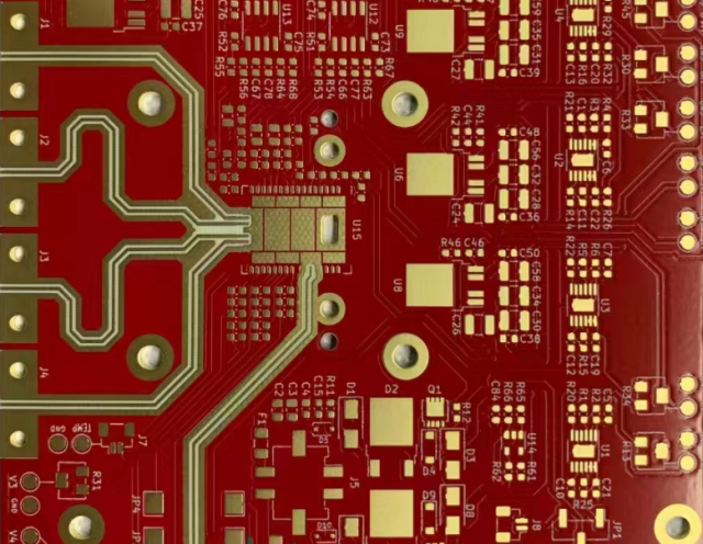
Design Considerations
Successful mixed signal IC test PCB design typically includes:
-
Optimized multilayer stackup separating analog, digital, and power layers
-
Dedicated analog and digital ground planes with controlled connection points
-
Short and symmetrical signal routing to reduce parasitic effects
-
Careful placement of decoupling and filtering components
-
Robust via design to minimize noise coupling
Close collaboration between PCB designers and test engineers is essential to achieve reliable mixed signal performance.
Materials Used in Mixed Signal IC Test PCBs
Material selection depends on signal speed and sensitivity:
-
High-TG FR-4 for standard mixed signal testing
-
Low Dk / Low Df laminates for high-speed digital sections
-
Hybrid stackups combining FR-4 and low-loss materials
-
Stable dielectric materials for consistent analog performance
Proper material selection helps maintain impedance accuracy and noise stability.
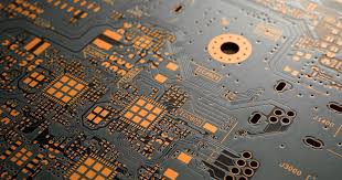
Manufacturing Capabilities
A professional mixed signal IC test PCB manufacturer should support:
-
Multilayer PCB fabrication (typically 8–24+ layers)
-
HDI PCB technology for dense routing
-
Controlled impedance manufacturing and validation
-
Tight tolerance drilling and registration
-
High-reliability surface finishes such as ENIG or ENEPIG
Precision manufacturing ensures repeatable electrical performance across test boards.
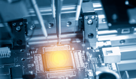
Assembly Considerations
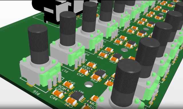
Mixed signal IC test PCB assembly often includes:
-
IC test sockets or DUT interfaces
-
High-speed digital connectors
-
Precision passive components for analog conditioning
-
Power filtering and reference circuits
Accurate assembly is critical to maintaining signal integrity and noise performance.
Applications of Mixed Signal IC Test PCBs
Mixed signal IC test PCBs are widely used in:
-
ADC and DAC testing
-
Power management IC (PMIC) testing
-
Sensor and interface IC testing
-
RF and mixed-signal IC validation
-
Automotive and industrial semiconductor testing
They are essential for verifying real-world performance of complex ICs.
Why Choose a Specialized Mixed Signal IC Test PCB Supplier
An experienced supplier provides:
-
Deep understanding of mixed signal test challenges
-
Optimized stackup and isolation strategies
-
Stable quality for repeated test cycles
-
Fast prototype and small batch production
-
Engineering support from design review to final assembly
Choosing the right partner improves test accuracy, reduces noise-related failures, and shortens development cycles.
